How To Write A Fast Matrix Multiplication From Scratch With Tensor Cores
- Introduction
- Background
- Kernels
- Conclusion
- Resources / Acknowledgements
Introduction
This post details my recent efforts to write an optimized matrix multiplication kernel in CUDA using tensor cores on a NVIDIA Tesla T4 GPU. The goal is to compute $D = \alpha * A * B + \beta * C$, as fast as possible. In this equation $D,A,B$ and $C$ are large matrices full of half precision floating point numbers, and $\alpha$, $\beta$ are constants. This problem is usually referred to as a Half-precision Generalized Matrix Multiply, or HGEMM for short.
Tensor Cores are specialized hardware units on NVIDIA chips that implement a small matrix multiplication in hardware. I recently became interested in tensor cores for two reasons. First, it seems like most generative AI training and inference these days happens on A100s and H100s. Second, all of this training and inference is almost certainly running on the tensor cores of these devices, because they offer a massive throughput increase for matrix math as compared to what you get if you dont use them. From here
An H100 GPU has 989 TFLOPs of half-precision matrix multiply compute, and ~60 TFLOPs of “everything else”. So, every cycle the tensor core is in use, you’re getting at least 94% utilization of the hardware. And every cycle the tensor core is not in use, you’re getting no more than 6% utilization of the hardware.
Given their huge importance in the world today, when I started this project it felt to me like there is disproportionately little info and dialogue on the internet about how to use them directly. I quickly learned this lack of dialogue on the internet is probably because writing algorithms that use them is a bit of a niche interest. The basic mechanics of how to call them are not hard, however writing a kernel that can use them at anywhere close their full potential is hard. Their huge throughput means that in order to use them at anywhere close to their full potential, you need to move bytes though the memory hierarchy of the GPU in a maximally efficient way, and overlap the computing with this data movement. There are certain algorithmic techniques that you need to use if you want get your moneys worth from your tensor cores, this article is an exploration of these techniques.
I figured out the implementation details mostly by digging around the NVIDIA CUTLASS forums and source, and I wrote this article in order to make sure I actually understand what I am doing, and also in the hope that some fellow GPU nerds trying to work with tensor cores might find it helpful. It should be noted that this whole project was done on a Turing architecture GPU, which was state of the art in 2018, and some details of some of the optimizations discussed in this article are somewhat specific to the Turing architecture. I noticed while working on this is that the more modern Hopper architecture has dedicated hardware support that directly addresses some of the performance issues and bottlenecks that I ran into along the way when working on optimizations that target an older GPU. More modern GPUs justify their increased price tag not only with increased floating point throughput, but also with features that ease the cognitive burden on programmers who are trying to optimize kernels for them.
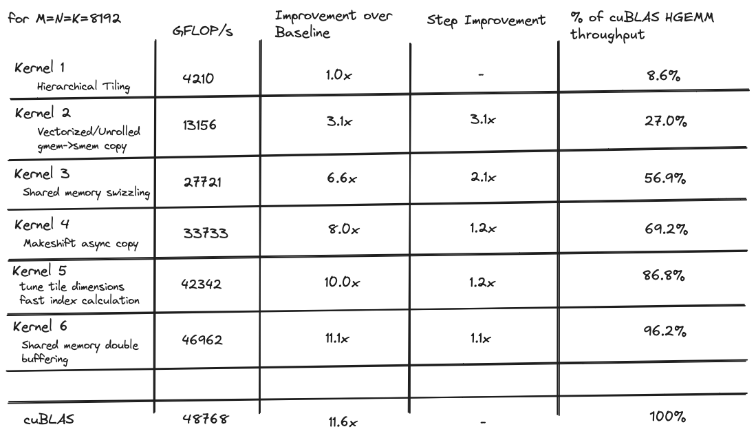
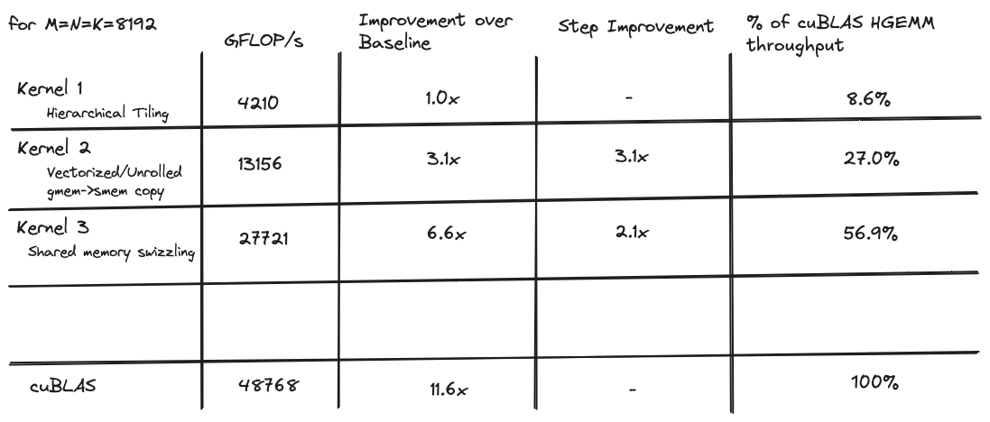
When I started my goal was to write a kernel with comparable performance to the cuBLAS hgemm implementation, which is the closed-source, gold standard implementation released by NVIDIA. I iteratively optimized a series of 6 kernels, with the first achieving a measly 8% of the cuBLAS throughput, and the last achieving a decent 96% of the cuBLAS throughput for 8192x8192 matrices.
This article contains a background section that explains some theory that is helpful to have in your head when thinking about how to optimize kernels that operate on matrices. The rest of the article explains six algorithmic techniques that I used to make my kernel run as fast as possible. Code can be found here on github, and here is a hacker news thread where you can leave comments.
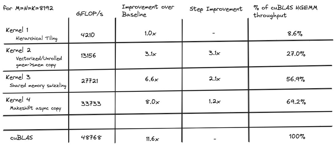
Here is a table with the performance comparison of all of the kernels:
Background
The memory wall
In the 70 or so years it has been since humanity started building transistor based computers, the capacity for performing arithmetic has been growing along the moores law exponential, while the capacity for moving data from where it is stored to where it is computed upon has not been growing exponentially. This problem is called the memory wall and it is one of the central problems in computer architecture today, especially when it comes to deep learning workloads, and especially especially when it comes to tensor core algorithms. What this means for us is that if we want to be able to use the ~65 trillion FLOPs per second that our tensor cores are capable of, moving the corresponding number of bytes per second from DRAM may be a challenge.
Roofline charts
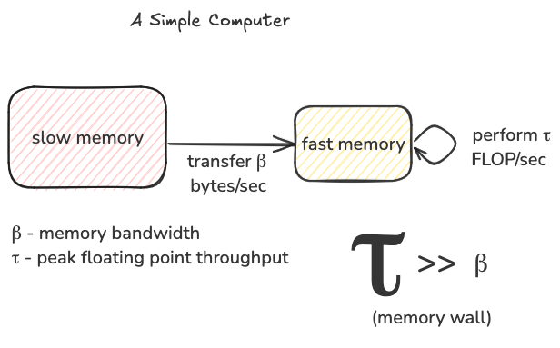
The roofline model allows us to think about this conundrum a bit more precisely. The basic idea is that we imagine a simplified computer with a two level memory hierarchy, fast memory and slow memory. We can only perform computation on data that is resident in fast memory, at a peak rate of $\tau$ FLOP/sec. The slow memory has unlimited size, and it can move $\beta$ bytes/sec of data into the fast memory. Because of the memory wall, $\tau$ is way larger than $\beta$.
Any given computation has a certain number of FLOPs that need to be performed, for example to multiply a $M$ by $K$ matrix with a $K$ by $N$ matrix we need to perform $2 * M * N * K$ FLOPs. The more FLOP/sec our algorithm can achieve, the faster we can get the matrix multiplication done. The roofline model gives us an upper bound on the FLOP/sec we can achieve, subject to $\tau$ and $\beta$ which are fixed properties of our hardware. We will refer to achieved FLOP/sec as $T$ for throughput, and the upper bound on T as $T_{max}$.
The maximum FLOP/sec we can achieve ($T_{max}$) is modeled as a function of a variable called computational intensity or $I$ for short, this is a property of the algorithm we write. This metric measures the “data reuse” of our algorithm in units of FLOP/byte: for each byte moved from slow memory to fast memory, how many FLOPs do we perform on it. According to the roofline model, if you are an algorithm designer, your primary concern is to write an algorithm with high computational intensity, or in other words to maximize $I$. In practice, this means moving a chunk of data from slow memory to fast memory, and then performing as many useful operations on it as allowed by whatever algorithm you are writing. Reusing data in fast memory is important for performance, because our memory bandwidth $\beta$ limited; it is a small number compared to $\tau$, which means the transfer of this chunk of data from slow to fast memory is costly. We make the most of it by performing as many useful FLOPs as possible on it.
The roofline model says the upper bound on FLOP/sec ($T_{max}$) we can achieve is the minimum of our computational intensity times memory bandwidth, and the peak floating point throughput of our hardware.
\[T_{max}=min(\beta * I, \tau)\]This model is saying there are two ways $T_{max}$ can be limited:
- $T_{max}$ can never exceed $\tau$. Even if we perform infinity operations on each byte we move into fast memory, we are still limited by the peak floating point throughput of the hardware. $\tau$ is typically a very big number, for example for the T4 GPU, $\tau$ equals 65,000,000,000,000 FLOP/second. If $\tau$ is our limiting factor, we are in good shape, this scenario is referred to as being compute bound.
- However, $T_{max}$ may also be limited by the memory bandwidth of the device, times the computational intensity of the algorithm. If $\tau$ were infinite, the achieved floating point throughput would simply be the number of bytes/sec being moved into fast memory, times the number of FLOPs performed per byte moved, this is $\beta * I$ (notice how when you multiply $\beta * I$, the units cancel out to give FLOP/sec). If $\beta * I$ is less than $\tau$, this term becomes the limiting factor on $T_{max}$, this scenario is referred to as being memory bound. The thing to do in this situation is to rewrite your algorithm to increase $I$ in the hopes of your algorithm becoming compute bound.
Here is the whole thing in a picture, notice how we can go from being memory bound to being compute bound by varying $I$:
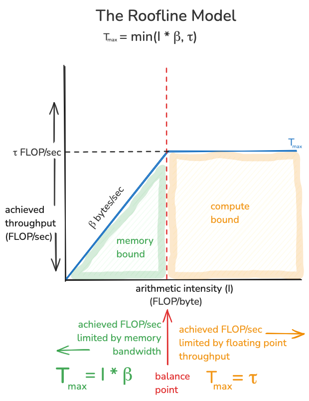
The red dotted line in this picture is referred to as the “balance point” of the hardware, it is the level of arithmetic intensity in units of (FLOP/byte) that we need to surpass in order to go from being memory bound to being compute bound. If we call this value $I^* $, then $I^* * \beta=\tau$ or equivalently $I^*=\frac{\tau}{\beta}$. It is a property of a particular computer, the peak floating point throughput, divided by the memory bandwidth. Because of Moore’s law, arithmetic throughput has been improving much faster than memory bandwidth, the consequence of this is that generally speaking, the newer the computer, the higher the balance point.
Rooflines for the NVIDIA Tesla T4
Plugging in some numbers specific to the GPU we are using, and looking at the resulting roofline can inform our algorithm design, and give us some perspective on what we are in for. On a real computer, there isn’t just a single $\tau$ and $\beta$, there are multiple hardware instructions, each with a different peak throughput $\tau$, and different types of memory, each with a different bandwidth $\beta$.
Tensor Core vs. FFMA
I found it helpful first to compare the balance point of the tensor cores with the balance point for the regular single precision math units, both with respect to global memory. This rooflines provides some intuition about why writing an efficient kernel is more challenging if you are using tensor core instructions, as opposed to the more standard, less specialized math instructions.
First, we need to know the global memory bandwidth $\beta_{gmem}$ of our device. NVIDIA spec sheets report theoretical memory bandwidth, which is never achievable in practice. The real number can be found with a benchmark, according to this whitepaper the achievable memory bandwidth of the T4 is 220 GB/sec (this is 68% of the 320 GB/sec theoretical memory bandwidth).
Next, we need to know the peak floating point throughput with the tensor core, and the peak floating point throughput without it. Similarly to memory, the theoretical numbers are not actually achievable without the GPU catching fire or melting. I find it reasonable to use the measured throughput of the cuBLAS half precision (uses tensor cores) and single precision (doesn’t use tensor cores) GEMM kernels as the achievable floating point throughput numbers. Looking at the assembly of the cuBLAS half precision kernel we can see that the grunt work is done by HMMA.1688, this instruction performs a single small hardware accelerated matmul (more on this later). For the single precision GEMM kernel, the instruction that does the work is called FFMA, this is a scalar multiply/accumulate operation, $d=a*b+c$. According to my benchmarks, the tensor core HMMA.1688 throughput is 49439 GFLOP/sec, which we will call $\tau_{HMMA}$. The non-tensor core FFMA throughput is 7455 GFLOP/sec, which we will call $\tau_{FFMA}$. These are respectively 76% and 92% of the theoretical peak throughputs, which seems reasonable enough. The resulting rooflines look like this (these plots are typically shown on a log/log scale, this one is not):
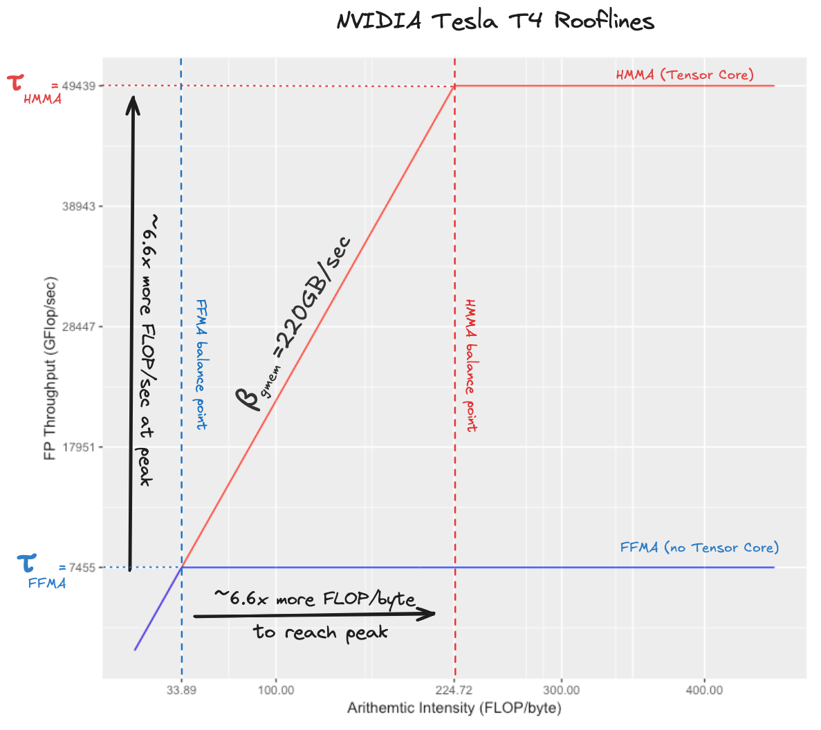
This plot should give us some intuition about the comparative hardness of writing a kernel that achieves peak FLOP/sec with tensor core instructions vs. writing a kernel that achieves peak FLOP/sec with fused multiply add instructions. The hardness comes from the fact that if we want to reach a throughput of $\tau_{HMMA}$, we need ~6.6x more arithmetic intensity than we need if our goal is to reach $\tau_{FFMA}$. The two balance points in this plot tell us that with FFMA instructions we can perform ~33 FLOPs in the time it takes a byte to travel from global memory, whereas with tensor cores we can perform 224 FLOPs in this same amount of time. This means that if we took a kernel that reached peak flops achievable with FFMA instructions, simply replacing the fused multiply adds in the inner loop with tensor core instructions would not be sufficient to get high tensor core utilization. We would additionally need to improve the code that moves data around to increase the computational intensity by a factor of six. This is one of the things that makes writing a tensor core GEMM interesting!
Shared memory vs. L2 cache vs. global memory
If we want to write a kernel that can make good use of the tensor cores, we need to be conscious of our computers memory hierarchy. The roofline model simplifies the memory hierarchy down to two storage types, one large and slow, and the other fast and instantaneous. In reality, there are more than two levels, each level has different a bandwidth and capacity, and also different considerations that must be considered in order to facilitate efficient access.
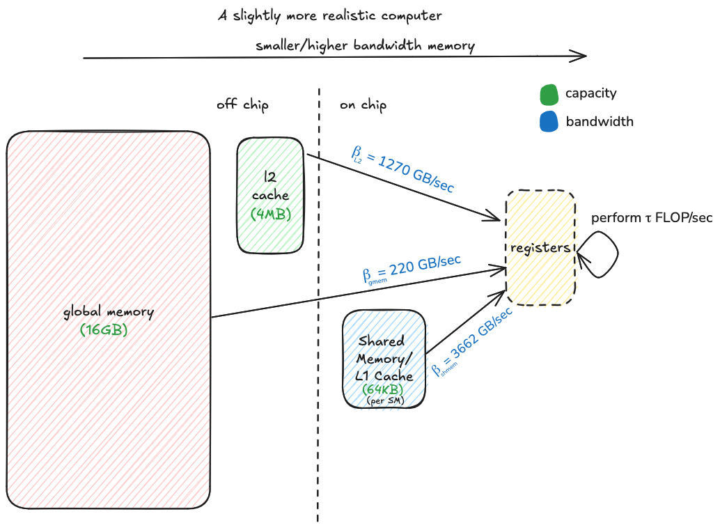
In these days of the memory wall, using the faster and smaller levels of the memory hierarchy effectively is critical. This requires some ingenuity because of the smallness: for example on the T4 the on chip shared memory has 16.6x the bandwidth of global memory, but on a given streaming multiprocessor (SM for short) it only fits 64 KiB. If we are multiplying large matrices, this is only enough space to fit a tiny portion of the problem.
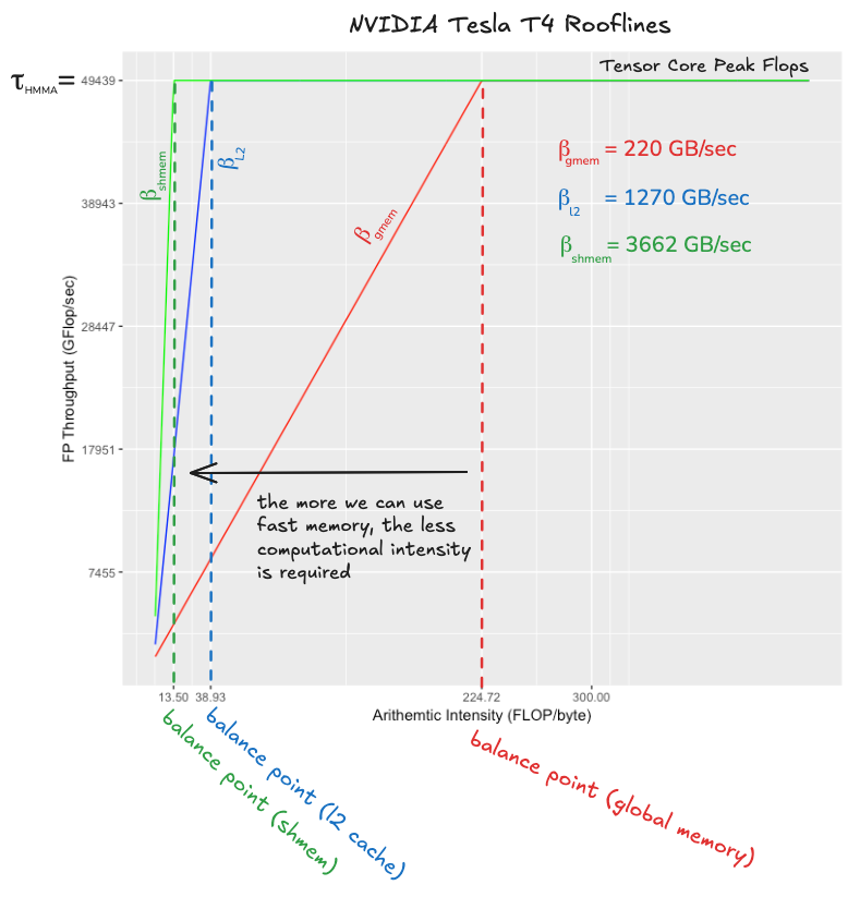
The plot compares the balance point of tensor cores with respect to:
- global memory or DRAM, the largest and slowest level of the memory hierarchy
- the L2 cache which stores recently accessed data from DRAM, and is shared between the 16 SMs on the T4
- shared memory, per SM fast memory that is explicitly managed.
Global memory has a balance point of 224, this means that if all of our memory accesses go to DRAM, we will need to perform 224 FLOPs for each byte read from DRAM in order to keep our tensor cores busy. This turns out to be a very tall order, as we will see later when we work out how parameters in our algorithm affect the balance point (the sneak preview is that given the amount of fast memory on the T4 and some other performance considerations, achieving this balance point would be counterproductive). However, the L2 cache comes to the rescue, its balance point with respect to tensor cores is 38, which is a much more manageable number. If a good number of our memory accesses can hit the L2 cache rather than going all the way to global memory, we will have a good shot at being compute bound rather than memory bound. The moral of this story is that we need the L2 cache.
Shared memory is used as an explicitly managed cache that will hold small portions of the input matrices local to a particular SM (a SM is kind of analogous to a single CPU core). Within the SM, threads will load their own local portion of the problem from shared memory into register memory, which is where data must reside in order for it to be computed upon. When shared memory is operating at full bandwidth, its balance point with respect to the tensor core is 13, which means we need to cache enough data in registers to perform 13 FLOPs for each byte read from shared memory. It turns out that each SM has enough register memory to make this easily achievable. When we are optimizing this part of the algorithm, the challenge will be to enable shared memory to operate at full bandwidth, which in practice means organizing the data layout in such a way that we can read it and write it without bank conflicts. Once shared memory is at full bandwidth, sufficient arithmetic intensity will be easy to achieve. I think the shared memory balance point of 13 is worth noting though, because it tells us that shared memory alone is not fast enough to achieve peak tensor core throughput. The moral of this story is that we need registers.
Theoretical arithmetic intensity
So modern computers generally have an imbalance between their arithmetic throughput and their memory bandwidth, consequently kernels that perform lots of arithmetic relative to data movement make better use of the hardware. At this point we need to think about the algorithm we are running, and forget about hardware for a moment.
Matrix Multiplication vs Matrix Addition
Any given algorithm has a maximum amount of arithmetic intensity that is possible, and our goal as an algorithm designer is to write a kernel that achieves an arithmetic intensity as close to this upper bound as we can manage. Comparing the maximum arithmetic intensity that is achievable when adding two $N$ by $N$ matrices, vs. multiplying them, illustrates how different algorithms have different upper bounds in this regard.
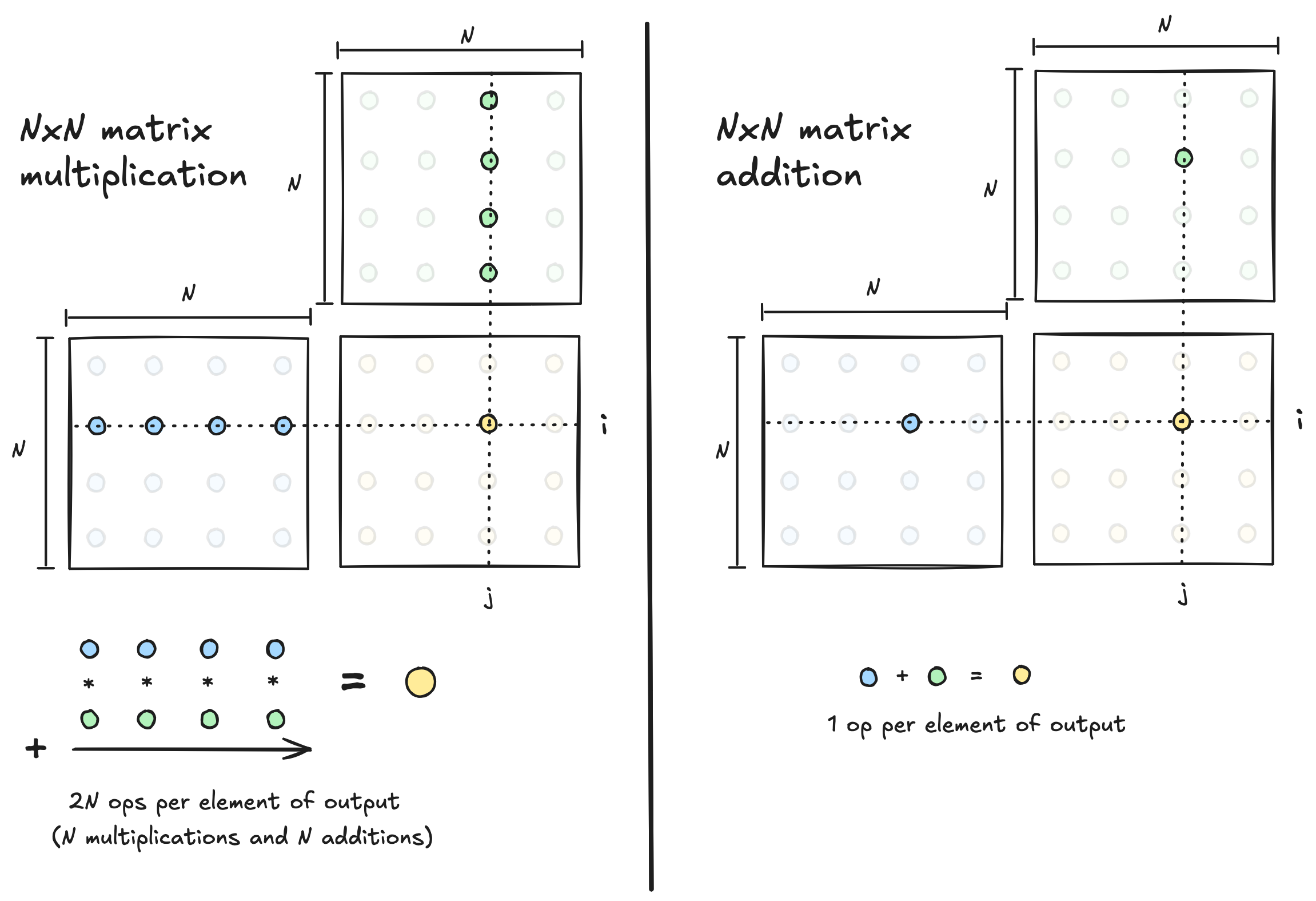
In the case of matrix addition, computing a single output element requires a single arithmetic operation, which means that when we run this algorithm the amount of data movement and compute will always be directly proportional. If we are adding two $N$x$N$ matrices, the amount of data involved is $O(N^2)$, and the amount of compute required is also $O(N^2)$. So the ratio of compute to data is $\frac{O(N^2)}{O(N^2)}=O(1)$, which means matrix addition will probably be memory bound on any modern device, regardless of how clever an algorithm we write. Relative to the amount of data movement, there just isn’t that much math required, so the upper bound on achievable arithmetic intensity is low. Lots of operations in deep learning fall into this low arithmetic intensity category, a technique called kernel fusion can be helpful here.
Matrix multiplication however is not doomed to be memory bound, because there is more arithmetic required relative to the problem size. When multiplying two $N$ by $N$ matrices, the amount of data involved is also $O(N^2)$, but the amount of compute required is $O(N^3)$ ($O(N)$ operations per output element, times $O(N^2)$ output elements). So the ratio of compute to data is $\frac{O(N^3)}{O(N^2)}=O(N)$. There is a factor of $N$ more compute required than data movement. The upper bound on the arithmetic intensity we can achieve grows with the matrix dimension $N$. If we are multiplying sufficiently large matrices, we should be able to write an algorithm that has sufficient arithmetic intensity to be compute bound rather than memory bound.
So in summary the arithmetic intensity we achieve depends on the kernel we write, and it must be less than or equal to an upper bound imposed by the algorithm our kernel is implementing. Achieved arithmetic intensity, given our machine parameters $\tau$ and $\beta$ determines whether we are memory bound or compute bound. If our algorithms upper bound on arithmetic intensity allows it, we want to optimize our kernel until it is compute bound rather than memory bound.
Achievable arithmetic intensity on a simple computer
For multiplying two $N$ by $N$ matrices, the best possible arithmetic intensity we can achieve is $O(N)$. Now the question is, how do we think about all of this when it comes time to actually write a kernel? To get at this question we need a model of the computer we are running on, to start out we will use the simple computer with fast and slow memory.
worst case
The first implementation of multiplication between two N x N matrices ($C=A*B$) on the simple computer looks like this. We load each value as soon as we need it, and store each output as soon as we are done with it. What is the ratio of compute to data movement? Is it close to the ideal of $O(N)$?
allocate registers a,b,c in fast memory
for i=1...N:
    for j=1...N:
        c = 0
        for k=1...N:
            load A(i,k) into a
            load B(k,j) into b
            c += a * b
        store c into C(i,j)
My mental model of this implementation looks something like this
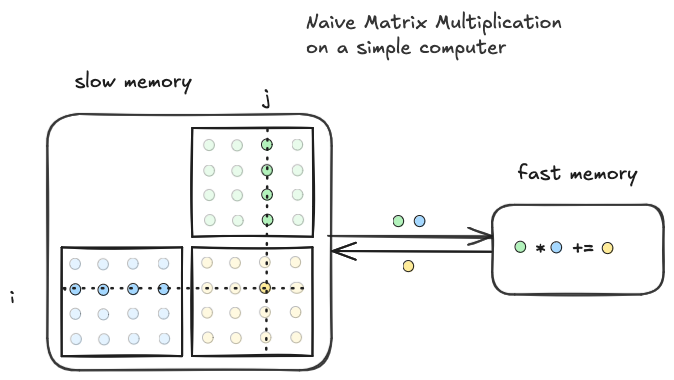
This arithmetic intensity of this implementation on the simple computer is $O(1)$, because on each iteration of the inner loop a single multiply/accumulate is performed, and only the data operated on during that iteration is loaded. There is $O(N^3)$ data movement, and $O(N^3)$ compute, which means $\frac{O(N^3)}{O(N^3)}=O(1)$ intensity, which is worse than the ideal by a factor of $O(N)$. This turns out to be the worst case.
best case
The poor intensity of the above implementation is the result of the fact that we load single elements from fast memory one at a time, only when they are needed. Only three matrix elements at a time are stored in fast memory. We can improve intensity by making better use of fast memory. To illustrate the best case scenario, imagine that fast memory was large enough to fit $A,B$ and $C$ in their entirety. If this were the case we could allocate space in fast memory for $C$, transfer the entire $A$ and $B$ upfront, perform the three nested loops with all the data already present in fast memory, and then once we are done store the entire $C$ matrix all at once back to slow memory.
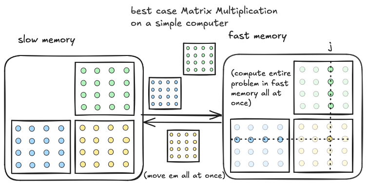 In this case, because we move each matrix only once, data movement is $O(N^2)$. Compute is the same as above, $O(N^3)$. Looking at the ratio of the two, we achieve the best case intensity, $\frac{O(N^3)}{O(N^2)}=O(N)$. However, this is unrealistic, because the entire problem will generally not fit in fast memory.
realistic case
We want to move more than three elements at a time between slow memory and fast memory. But we can’t move the full matrices all at once. We can compromise by moving subtiles of $A$ and $B$ from slow memory to fast memory (as large as we can fit). Each pair of input tiles we move to fast memory corresponds to a tile of the output which can be computed with a mini matrix multiplication between the input tiles we have resident in fast memory. We then move the next pair of input tiles to fast memory and then compute again.
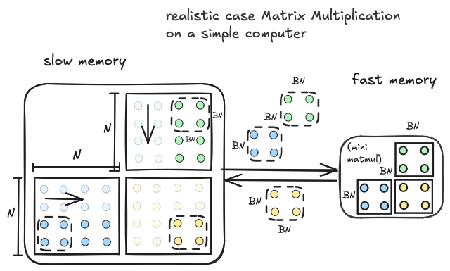
Here is some pseudocode corresponding to the above diagram:
Allocate A_tile[BN, BN], B_tile[BN,BN], C_tile[BN,BN] in fast memory

# outer loop over tiles of A and B
for i=1...N in steps of size BN:
    for j=1...N in steps of size BN:
        C_tile[: , :] = 0
        for k=1...N in steps of size BN:
            Load A[i : i+BN, k : k+BN] into A_tile
            Load B[k : k+BN, j : j+BN] into B_tile

            # inner loop, do a mini matmul between tiles of A and B
            # store the result in C_tile
            for tile_i=1...BN:
                for tile_j=1...BN:
                    for tile_k=1...BN:
                        C_tile[tile_i, tile_j] +=
                            A_tile[tile_i, tile_k] * B_tile[tile_k, tile_j]

        # once we have looped over all the tiles along the K dimension of A,B
        # store C_tile back to its place in slow memory
        Store C_tile into C[i : i + BN, j : j+BN]
What is the ratio of compute to data movement? How does it compare to the worst cast and the best case? We can answer these questions by looking at the loop structure.
Lets think about data movement first. There are three nested loops on the outside, each of which go from $1$ to $N$ in $BN$ sized steps. Each loop iterates $\frac{N}{BN}$ times, and since we have three levels of nesting, whatever is inside the nested loop body will happen $(\frac{N}{BN})^3$ times. Inside the loop nest, we load two tiles of size $BN^2$, one corresponding to each of the input matrices. Asymptotically this works out to $O((\frac{N}{BN})^3 * BN^2)$ data movement (we can ignore the storing of the C_tile, since this is only inside two of the loop nests, it only happens $\frac{N}{BN}^2$ times). Cancelling things out gives us $O(\frac{N^3}{BN})$ data movement. Notice that this a factor of $BN$ less data movement than the naive case.
Now compute. Same as above, we have three nested loops, the inside of this loop body will execute $(\frac{N}{BN})^3$ times. Inside the loop nests, the compute consists of the mini matmul between two $BN$ by $BN$ tiles, the three nested loops have a total of $O(BN^3)$ steps what is what we expect for multiplying together two $BN$ by $BN$ matrices. So the total amount of compute is $O((\frac{N}{BN})^3 * BN^3)$ which simplifies to just $O(N^3)$. This is the number of steps we expect for multiplying two $N$ by $N$ matrices, and it is the same as the naive case.
So this tiled approach has the same number of compute steps as the naive implementation, but a factor of $O(BN)$ less data movement. The arithmetic intensity works out to $O(\frac{N^3}{\frac{N^3}{BN}})=O(BN)$. In english, this is telling us that our achieved arithmetic intensity will scale linearly with the dimension of the tiles that we are fitting in fast memory.
In Summary
The final takeaway is fairly intuitive. The best possible intensity we can achieve when multiplying two $N$ by $N$ matrices scales with the matrix dimension $N$. However, achieving this upper bound would require fitting the entire $O(N^2)$ sized problem in fast memory, which wont be possible. So we compromise by breaking down the $O(N^2)$ sized problem into lots of smaller $O(BN^2)$ sized problems, and we choose $BN$ such that all of our fast memory is filled up. The intensity we can then achieve scales with $BN$. So in practice, the intensity we can achieve is limited by the size of fast memory on our device.
Parallelized matrix multiplication on a GPU
Thinking about matrix multiplication on the simple computer helps build intuition about how using the memory hierarchy to our advantage can result in higher arithmetic intensity, which will help for maximizing the performance of our kernel. However the simple computer model is a bit too simple, it consists of a two level memory hierarchy and some compute that can operate at a rate of $\tau$ on the data in fast memory. Our goal is to write a fast matrix multiplication kernel that will run on a GPU, which raises the question of how a GPU is different from the simple computer.
On the most fundamental level that answer is that GPUs, like the simple computer, have a memory hierarchy. But on a GPU the memory hierarchy fits within a hierarchy of concurrent compute units. Here is a diagram of a simple GPU that illustrates this.
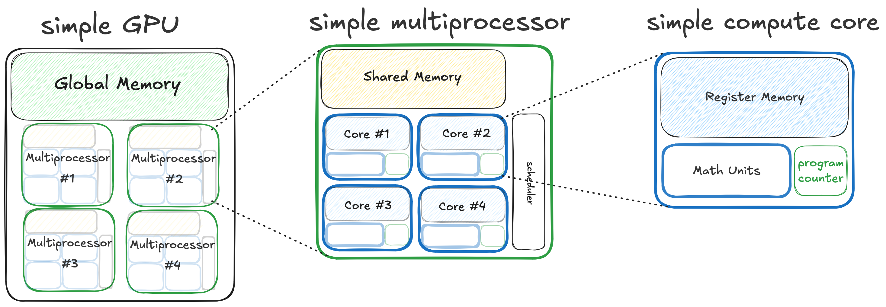
On the simple GPU there are three levels to the combined compute/memory hierarchy.
- At the highest level is the whole GPU, which owns a big piece of DRAM (global memory). The GPU is composed of four multiprocessors, each of which are independent units of a compute, run concurrently with respect to each other and can all read/write to the same DRAM.
- At the middle level there is a multiprocessor which owns a piece of SRAM (shared memory), and is composed of four cores which are independent units of compute that run concurrently and can all read and write the same shared memory that is local to the multiprocessor.
- At the lowest level is a single compute core which owns some private register memory, and can execute a single thread and perform arithmetic independently of the rest of the computer.
Hierarchical Tiling (simple gpu)
So how do we use this type of computer to perform a matrix multiplication? The first useful observation is that the matrix multiplication problem can be broken down hierarchically into nested tiles. This is good news, because a hierarchical algorithm is a good fit for a hierarchical computer.

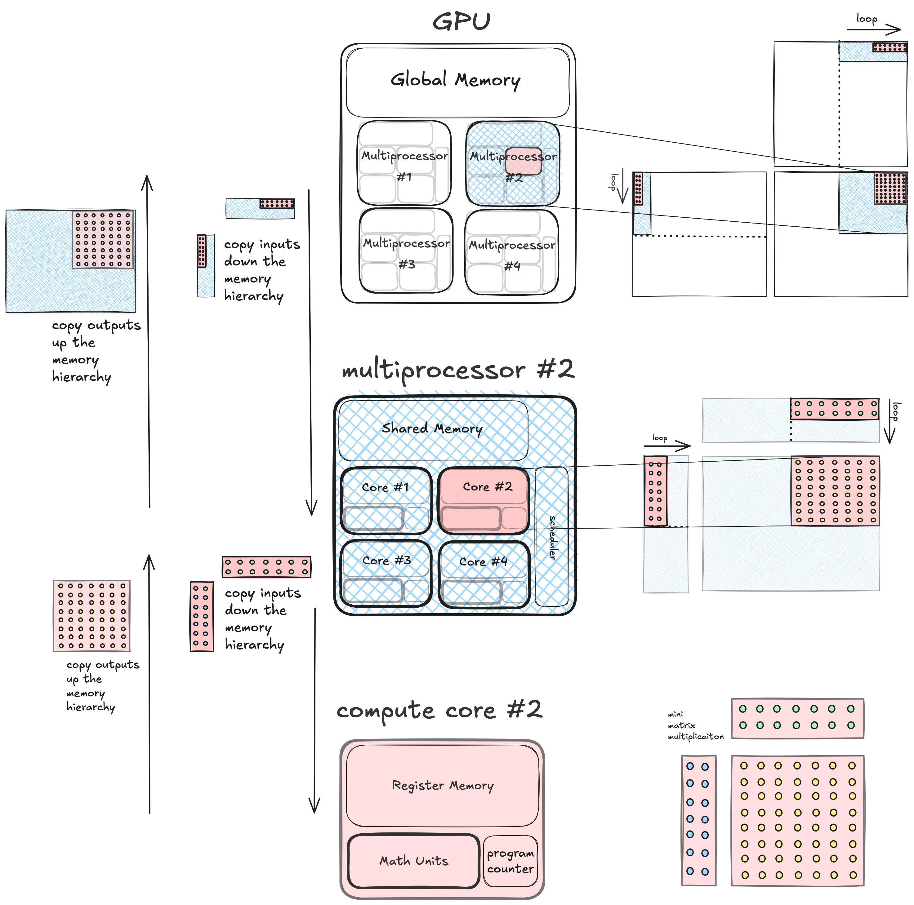
If we are computing a matrix multiplication $C=A*B$, we can divide the output matrix $C$ into non-overlapping tiles, and assign each tile to a compute unit. Each of these output tiles can then be computed with a matrix multiplication between corresponding tiles of the input, independently of the other tiles. Since our machine is hierarchical, there are compute units within compute units, and correspondingly there are matrix multiplications within matrix multiplications. We recursively break down the problem into nested tiles, until we end up at an atomic element of compute which physically is usually a single core of some sort, and logically is a single thread of execution. At this level the single thread computes a small matrix multiplication between its tiles of the input.
Hierarchical Tiling (real gpu)
The above diagram shows a coarse, high level view of what a GPU implementation of hierarchical tiling looks like. When implementing this in CUDA for an NVIDIA GPU, there are some finer details we need to fill in. This tiling structure is created by:
- a series of global, shared, and register memory allocations of fixed dimension
- nested loops which control the positions of the tiles
- synchronization points between threads running within a multiprocessor
- compute at the lowest level, which in this case is a small matrix multiplication that runs on the tensor core
This kernel was my starting point, but if you are interested in reading about a series of 10 kernels which build up to one like this, I recommend reading this.
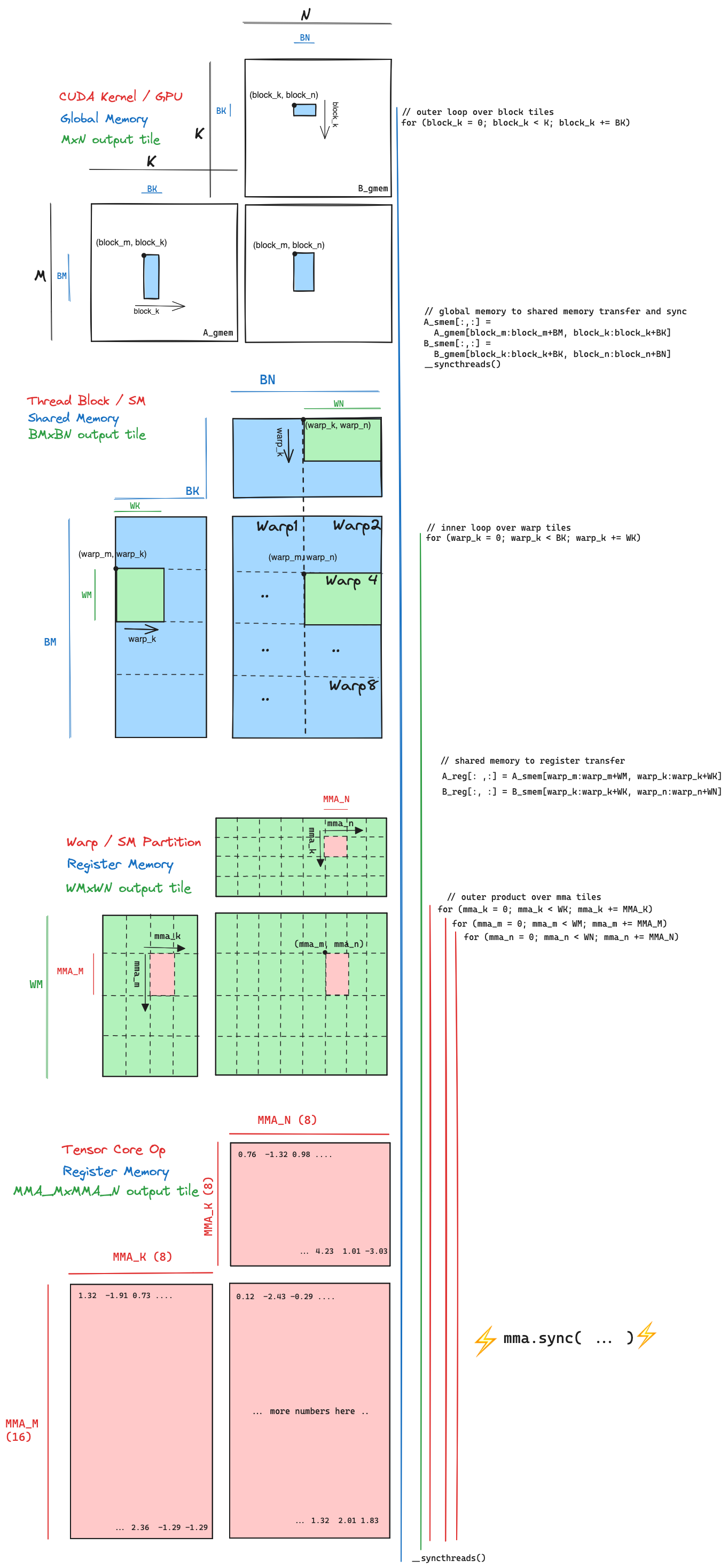
With this diagram my attempt is to show the correspondence between loop nests and the tiling structure. There are four levels, each level corresponds to a level of the compute hierarchy, memory hierarchy, and tile shape.
Here is a quick description of each level from the perspective of the compute unit relevant for that level:
-
CUDA Kernel / GPU level: The GPU is reading the three input matrices, $A$, $B$, and $C$ from global memory, and writing the output matrix $D$ to global memory. Each thread block is looping over the
Kdimension (aka the ‘inner’ dimension) of $A$ and $B$. This loop is incrementingblock_kin steps of sizeBK. At each iteration we are copying the blue blocktiles from global memory to shared memory. -
Thread Block / SM level: At this point the blue subtiles of $A$ and $B$ that a particular thread block needs to compute a
BM,BNtile of the output have been copied into shared memory. This thread block is running on one of the 16 SMs on the GPU, and the shared memory is local to that SM and fast to access. Within the thread block there are 256 threads, which is 8 warps containing 32 threads each. Within the thread block, theBM,BNtile of the output is partitioned 8 ways, so that each of the 8 warps can work concurrently on the compute. Each of the warps is looping over the inner dimension within the block tile, this loop is incrementingwarp_kin steps of sizeWK. At each iteration we are copying the green warp tiles from shared memory to register memory. -
Warp / SM Partition: At this point the green warp tiles within the blue block tiles have been copied into register memory, and it is the responsibility of a particular warp, running on one of the 4 partitions on the Turing SM to compute the
WMbyWNtile of the output. Each warp computes its tile of the output by taking an outer product between theWM,WKtile of A and theWK,WNtile of B. Inside the three nested loops that compute the outer product, the we an MMA sync operation. -
Tensor Core Op: Finally we get down to the last level of the hierarchy, which is a single tensor core op, this is a single hardware accelerated (16,8) x (8,8) = (16,8) matrix multiply that takes place in and out of register memory.
Performance considerations on a real GPU
When implementing this structure in a CUDA kernel that targets a particular GPU architecture, there are a number of things that must be considered given that we are trying to squeeze every last drop of performance out of the hardware. I divide the performance considerations into three buckets, each optimization discussed in the rest of this article falls into one or two of these buckets.
Arithmetic intensity as a function of tile dimensions
The necessity of achieving high arithmetic intensity is why we have this structure of tiles within tiles, and the tile dimension is the primary knob we can turn that determines the arithmetic intensity of our kernel. In our kernel we are first loading data from global memory to shared memory, and then shared memory into registers. In both cases we are loading two rectangular tiles corresponding to the input data from slower memory to faster memory, and then eventually computing a matrix multiplication between these two inputs at the lowest level of the hierarchy. The arithmetic intensity we should achieve is a function of the tile dimensions we choose (larger is better), this is worked out below.
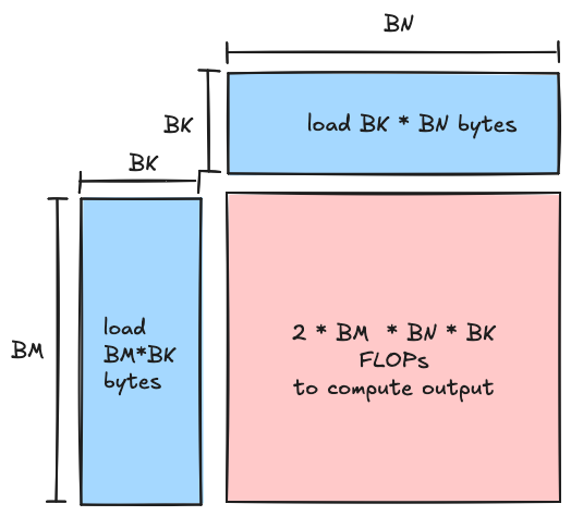
- FLOPs: At each iteration of the inner loop, each thread block multiplies a $(BM,BK)$ shaped matrix with a $(BK,BN)$, to produce a $(BM,BN)$ tile of the output. This matrix product consists of $2 * BM * BK * BN $ FLOPs (three nested loops over the dimensions, with a multiply and accumulate operation in the inner loop)
- memory: The $(BM,BK)$ and $(BK,BN)$ shaped matrices are read from global memory each iteration, since each element is two bytes this comes out to a total of $2(BM * BK + BK * BN) = 2BK(BM + BN)$ bytes read, and we don’t perform any writes in the inner loop, all writes happen in the kernel epilogue.
Taking the ratio of these two, the arithmetic intensity we should achieve for a given block tile size works out nicely to $\frac{BM*BN}{BM+BN} \frac{FLOP}{byte}$. For the thread block level tiles at the second level of the hierarchy, we will want to choose our tile dimensions such that this ratio is larger than the balance point of the tensor cores with respect to global memory, but we will be limited by the size of shared memory. Likewise for the warp tiles at the next level down in the hierarchy, we will want to choose the tile dimensions such that this ratio is larger than the balance point of the tensor cores with respect to shared memory, but we will be limited by the size of register memory. The former turns out to be a bit more challenging than the later.
Overlap between compute and data movement
The roofline model gives us an upper bound on arithmetic throughput $T_{max}=min(\beta * I, \tau)$. In order to achieve this upper bound, we need perfect overlap between compute and data movement. In order to see why this is, imagine we achieve an arithmetic intensity sufficient to put us in the compute bound regime of the roofline model. At this point in order for our achieved throughput to actually equal the upper bound $T_{max}=\tau$, we need to be continuously computing, any time that our compute spends idle will mean that our achieved throughput is less than the machine peak $\tau$. There are a number of reasons why our compute will spend periods of time idle, such as memory latency, data dependencies, and synchronization points.
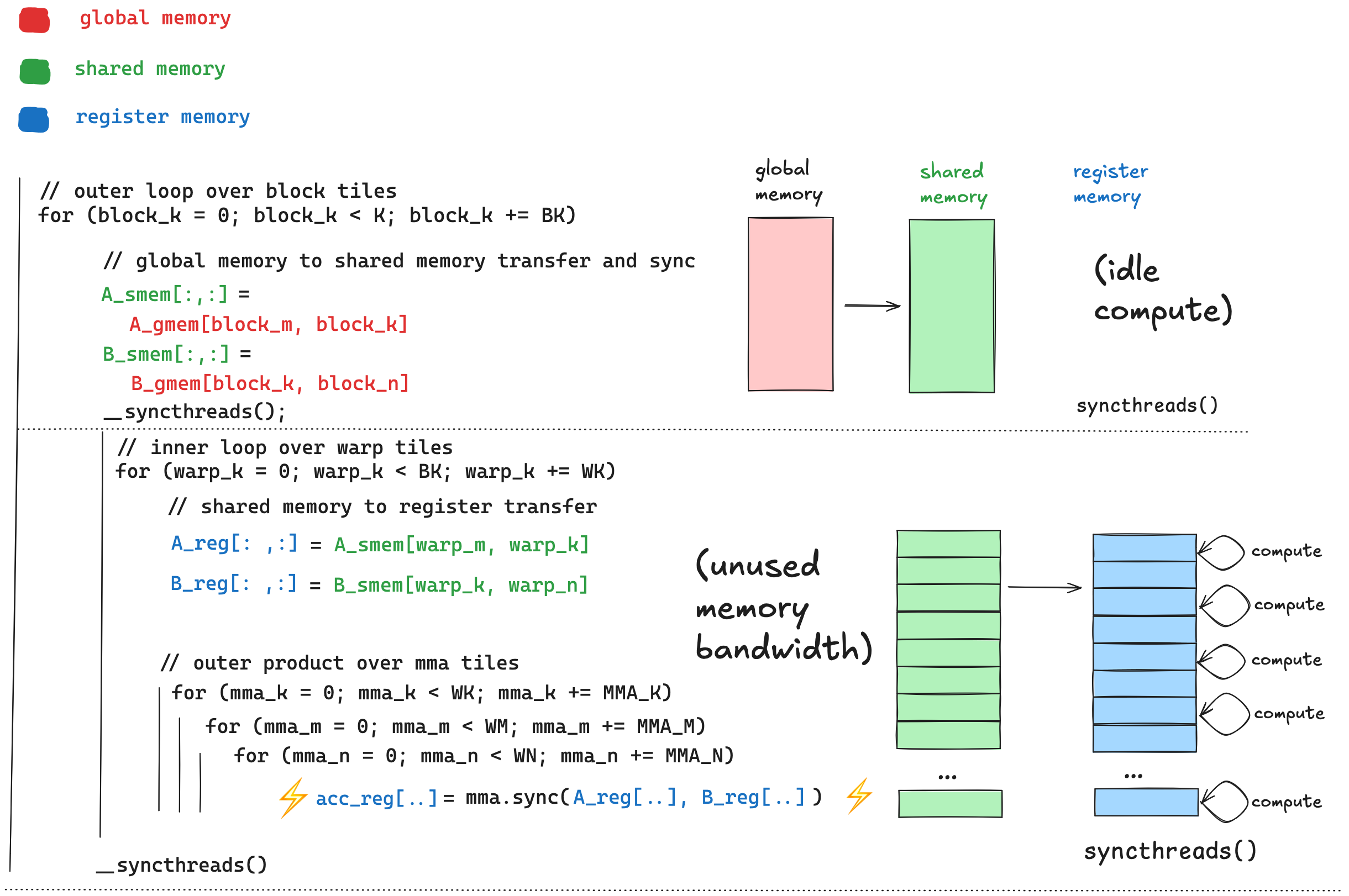 As illustrated above our initial loop structure has some inefficiencies in this regard.
Maximizing memory bandwidth
According to unofficial benchmarks the best achievable global memory bandwidth on the T4 is ~220 GB/sec, and the best achievable shared memory bandwidth is ~3662 GB/sec. However, an unoptimized kernel will only achieve a fraction of these numbers. The first consideration is access pattern; when groups of adjacent threads are requesting memory, some mappings of threads to data in memory are more efficient than others. The hardware that implements global memory vs. shared memory functions differently, consequently an access pattern that is optimal for reading shared memory may not be optimal for reading global memory.
The main consideration for global memory access is called coalescing, the one sentence summary is that maximum global memory bandwidth is achieved when adjacent threads access adjacent data in global memory (explained here). Shared memory is dove into in a later chapter.
How to use Tensor Cores
This section is a brief overview of the mechanics of using tensor cores.
All tensor core operations are performed at the warp level in the compute hierarchy; 32 threads collaboratively load data into their registers and then synchronously execute a small hardware accelerated matrix multiply. When thinking about tensor core algorithms, we should think of the warp as an atomic element of compute, even though in reality a warp contains 32 threads capable of doing their own thing. By comparison if we were writing GEMM kernel without tensor cores, individual threads performing scalar multiply accumulate operations would be our atomic element of compute.
Tensor cores are accessible via two different methods. The first is via the wmma api which is part of the CUDA toolkit. wmma seems to be regarded as the more portable and less performant way to program tensor cores. I gave up on it pretty quickly, as it abstracts away the loading of input data from shared memory into register memory, and it turns out there are some details here which are critical for performance.
The other route is to use the mma family of instructions which are part of PTX, this option is more flexible and performant than the wmma route. PTX is an intermediate representation for NVIDIA GPUs that is lower level than CUDA, but higher level than SASS (this is the assembly language that NVIDIA GPUs run). PTX can be inlined in a kernel in order to call tensor cores.
The PTX instruction I used is mma.sync.aligned.m16n8k8.row.col.f16.f16.f16.f16 (documentation here), each part of this instruction means something:
-
mma: we are performing a matrix multiply accumulate operation -
sync: this instruction is synchronous, all 32 threads will wait until all 32 threads are done before resuming execution -
aligned: all 32 threads in a warp must execute this instruction, if less than 32 threads in a warp were to execute this instruction, behavior is undefined -
m16n8k8: this is the identifier for the matrix fragment shape. This means the fragment of matrix $A$ has shape (16,8), the fragment of $B$ has shape (8,8), the fragments of $D$ and $C$ have shape (8,8). (Remember, the formula for a GEMM is $D = \alpha * A * B + \beta * C$). If you look at the PTX documentation linked above, there are lots of different shapes to choose from, however the Turing/Volta architectures only support a limited number. Ampere supports more, and Hopper supports even more. -
row: the $A$ fragment should be stored in registers in a row-major layout -
col: the $B$ fragment should be stored in register in a column-major layout -
f16: $D$ is an fp16 matrix -
f16: $A$ is an fp16 matrix -
f16: $B$ is an fp16 matrix -
f16: $C$ is an fp16 matrix
Each mma.sync instruction expects a specific layout of fragment elements across the registers of the 32 threads in a warp, these layouts can be found in the PTX docs. Here is the m16n8k8 layout:
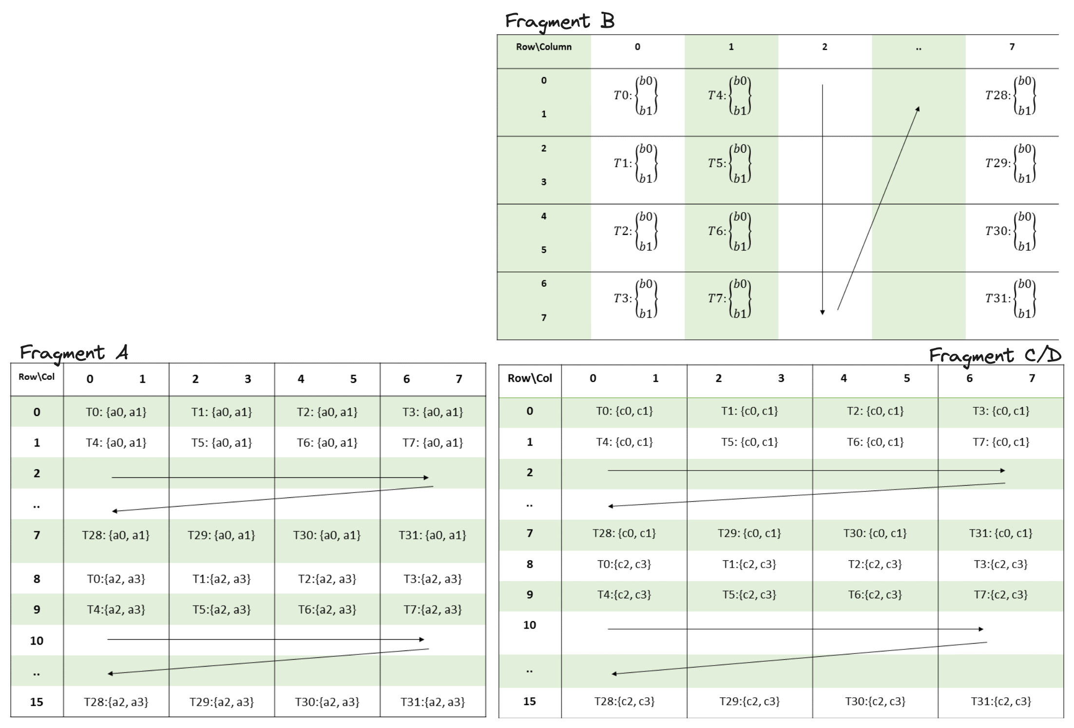
These diagrams are describing a mapping between threads, registers, and matrix elements:
-
T0, T1, T2 ...refers to the index of the thread. Thread indices in these diagrams range from 0-31 since there are 32 threads in a warp. -
a0, a1, a2, ... b0, b1, b2, ... c0, c1, c2refer to registers that hold matrix elements. - The position of each thread/register pair tells us which matrix elements go in which registers of which thread. For example,
T0: {a0,a1}is at the top left corner of matrix fragment A, this means elements(0,0)and(0,1)in this fragment are placed in registersa0anda1of thread 0.
Luckily there is another PTX instruction called ldmatrix (docs here) which loads a rectangular tile of data from shared memory, and shuffle matrix elements within a warp in order to create this layout for us. It can optionally transpose matrix elements as it moves them from shared memory to register, which is convenient for matrix B above, which is in a column major, or “transposed” layout.
The inner loop our our kernels will consist of repeatedly calling ldmatrix to move data from shared memory into register memory, and then repeatedly calling the m16n8k8 variation of mma.sync in order to multiply tiles together with the tensor core. For this project I used a Turing architecture GPU, on Ampere the tensor core API is very similar, but with more matrix shapes supported. On Hopper, the API is expanded substantially, PTX instructions are introduced that allow a group of 128 threads to asynchronously execute a much larger matrix multiplication than m16n8k8.
Kernels
For the rest of this article I will discuss a series of kernels that got me to ~96% of cuBLAS level performance on a tensor core GEMM, for 8192x8192 matrices. Each kernel builds on the previous one, and the themes of each are:
- hierarchical tiling
- vectorized/unrolled gmem->smem transfer
- shared memory swizzling
- makeshift async copy
- tune tile dimensions
- optimized index calculation
- double buffering
Kernel 1 - Hierarchical Tiling
The first kernel I wrote is an implementation of the hierarchical tiling structure shown above. Here is pseudocode for the loop structure that performs the matrix multiplication.
// outer loop over block tiles
for (block_k = 0; block_k < K; block_k += BK)
{
    // global memory to shared memory transfer
    A_smem[:,:] = A_gmem[block_m:block_m+BM, block_k:block_k+BK]
    B_smem[:,:] = B_gmem[block_k:block_k+BK, block_n:block_n+BN]

    // synchronize across the thread block in between
    // writing shared memory and reading shared memory
    __syncthreads();

    for (warp_k = 0; warp_k < BK; warp_k += WK)
    {
        // load from shared memory into register memory in preparation for compute phase
        A_reg[: ,:] = A_smem[warp_m:warp_m+WM, warp_k:warp_k+WK]
        B_reg[:, :] = B_smem[warp_k:warp_k+WK, warp_n:warp_n+WN]

        // outer product over mma tiles
        for (mma_k = 0; mma_k < WK; mma_k += MMA_K)
        {
            for (mma_m = 0; mma_m < WM; mma_m += MMA_M)
            {
                for (mma_n = 0; mma_n < WN; mma_n += MMA_N)
                {
                    mma_sync_m16n8k8(
                        acc_reg[mma_m:mma_m+MMA_M, mma_n:mma_n+MMA_N],
                        A_reg[mma_m:mma_m+MMA_M, mma_k:mma_k+MMA_K],
                        B_reg[mma_k:mma_k+MMA_K, mma_n:mma_n+MMA_N],
                        acc_reg[mma_m:mma_m+MMA_M, mma_n:mma_n+MMA_N]
                    )

                }
            }
        }
    }
    __syncthreads();

}
The 8% of cublas throughput it achieves is the starting point. The rest of this article delves into some techniques I used to make it faster.

Kernel 2 - Vectorized memory copy and loop unrolling
In order to improve the performance of our code, we need to know why it is slow. When writing CUDA kernels, the best tool to use for this is called NSight Compute, a profiler developed by NVIDIA that gives lots of detailed metrics about what is happening in hardware while a kernel executes. The first place I typically look is the section called “Warp State Statistics”. As a kernel is executing, each warp is being issued instructions by a scheduler. In an ideal world, the scheduler would be able to issue a new instruction each clock cycle. In the real world, it is very hard to write a kernel that can issue a new instruction every cycle, there are all sorts of reasons why on a given cycle, a warp may not be capable of executing its next instruction and will instead “stall” i.e. do nothing. The reasons for stalling can be due to capacity limits of various hardware pipelines, memory latency, or synchronization points in our kernel which require all the threads running on an SM to wait for all the other threads to catch up. The Warp State Statistics section tells us how many clock cycles the average warp spends stalled, per average instruction issued, broken down across a bunch of different categories. This gives us the information we need to target our optimizations to the least performant parts of our kernel. Here is a screenshot of what the Warp State section for Kernel 1.
 The “Warp Cycles Per Issued Instruction” field tells us that on average for each instruction issued, warps spend about ~30 cycles idle, and the table below tells us that 16 of these 30 cycles are due to the “Long Scoreboard” stall category.
Scoreboarding is an algorithm implemented in the hardware of most processors for tracking when the data dependencies for the next instruction have arrived in the registers they need to be in for the instruction to execute. Most modern CPUs are able to reorder instructions on the fly such that instructions whose operands are ready can execute ahead of instructions whose operands have yet to arrive in registers. The reordering is done in hardware, subject to constraints imposed by the data dependencies between subsequent instructions. This is called out of order execution and it is a rather fancy technique for hiding latency. GPUs do not reorder instructions as they are executing, I would imagine because the logic required consumes a fair amount of precious transistors on the chip, and since GPUs are designed for throughput these transistors are better spent on things like tensor cores.
GPUs do however track data dependencies, but with a lot more help from the compiler as compared to CPUs. When the data required to execute the next instruction has not arrived in register memory, the warp that is executing just waits for its data to arrive. The “Long Scoreboard Stall” approximates the average number of cycles that warps spend stalled waiting for data dependencies. The fact that this stall reason accounts for ~50% of all the cycles that warps spend idle tells us that the performance of Kernel 1 is primarily limited by memory latency. This tells us we should focus on the code that is moving data from global memory onto the chip, and figure out how to minimize the latency per byte moved.
Reading a rectangular tile of data from global memory, and writing it to shared memory is the first thing that occurs on each iteration of the outer loop of the kernel. The easiest way to do this is for adjacent threads to access adjacent values in global memory, and write data to shared memory in the same layout that it came from in global memory. This access pattern is optimal both for reading global memory, and writing shared memory. Here is the first data transfer that I wrote:
__device__ void tileMemcpy(
    half* src,
    half* dst,
    const unsigned int src_stride,
    const unsigned int tile_rows,
    const unsigned int tile_cols
)
{
    // flatten out 2d grid of threads into in order of increasing threadIdx.x
    const unsigned int thread_idx = threadIdx.y * blockDim.x + threadIdx.x;
    const unsigned int num_threads = blockDim.x * blockDim.y;

    // # of threads is multiple of # of columns in the tile
    assert(num_threads % tile_cols == 0);

    // assign each thread a row/column in the tile, calculate the row step
    const unsigned int row_step = num_threads / tile_cols;
    const unsigned int thread_row = thread_idx / tile_cols;
    const unsigned int thread_col = thread_idx % tile_cols;

    for (unsigned int r = thread_row; r < tile_rows; r+=row_step)
    {
        dst[r * tile_cols + thread_col] =  src[r * src_stride + thread_col];
    }
}
Looking at the SASS corresponding to this tileMemcpy function in godbolt, we can see that the copy operation inside the loop dst[...] = src[...] compiles to two operations from the lower level perspective of SASS, a two byte load from global memory (LDG.U16 in SASS), followed by a two byte store (STS.U16), along with a bunch of index calculations and loop overhead. The long scoreboard stall prevents the store from taking place until the value we are loading has arrived in the register.
Here is a visualization of how this loop is executing, for a single thread:
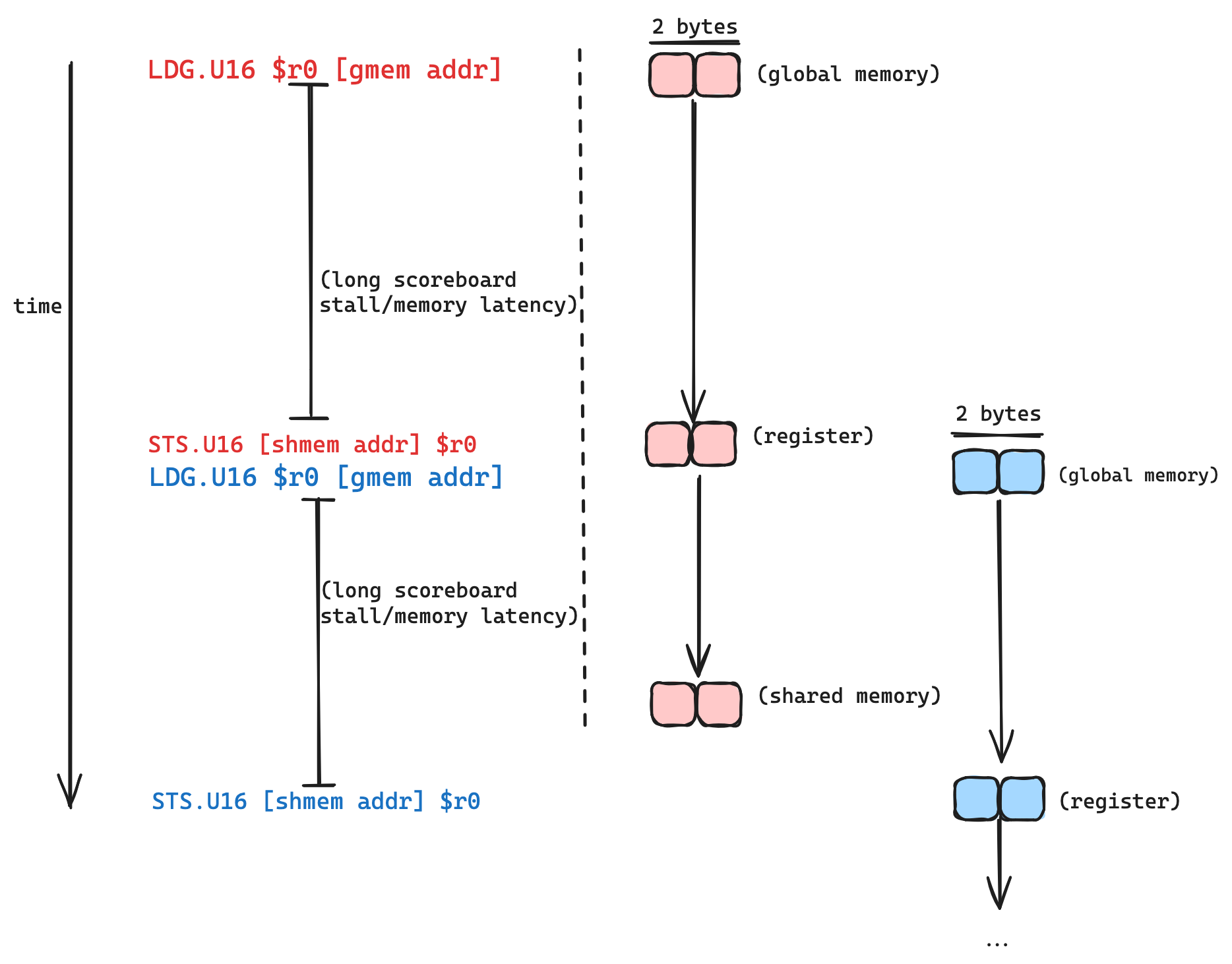 Latency in between the load and the store is inevitable: a request is sent to a DRAM controller, data is fetched from DRAM and then transmitted over bus. Unless we hack the laws of physics or invent a time machine we can’t get rid of the latency. But what we can do is hide it.
Latency hiding is a central concept in computing, and at its core is very simple. It just means that if we are performing an operation $X$ that has some latency, we want to be doing other useful work while $X$ is happening, rather than wait and do nothing. For example, if I wake up and decide I want an omlette, I would first turn on the burner and let the pan warm up, and while that is happening I would crack the eggs and grate cheese. This order of operations hides the latency of warming up the pan with the cracking of eggs and grating of cheese. If I am hungry and eager to eat the finished omlette as soon as possible, it would be silly to idly stand there and watch as the pan warms up.
The same principle applies to hiding the latency of the global memory loads in tileMemcpy. Since the copy operation is happening inside a loop, each thread is performing multiple loads and multiple stores, in an order like load (stall) store, load (stall) store, .... What if we were able to rearrange these so that the order is load load load (stall) store, store, store. In this later ordering the data requested by the three loads will be in flight at the same time, and we can say that the latency of each load is being hidden by the other loads. The easiest way to accomplish the later ordering is by unrolling the loop in tileMemcpy. If we can unroll the loop, nvcc should be smart enough to reorder the instructions so that the global memory loads are hiding each others latency. In this case the compiler is doing for us what a CPU would do in hardware on the fly.
If we want to unroll the loop, the number of loop iterations must be known at compile time. The number of loop iterations is a function of the number of threads per block, and the block tile dimensions. Both of these are fixed at compile time, so passing them as template parameters into tileMemcpy and calculating the number of iterations as a function of these, and adding a #pragma unroll does the trick.
template<unsigned int TILE_ROWS,
unsigned int TILE_COLS,
unsigned int NUM_THREADS>
__device__ __forceinline__ void tileMemcpyUnrolled(
    half* src,
    half* dst,
    const unsigned int src_stride
)
{
    // # of threads is multiple of # of columns in the tile
    static_assert(NUM_THREADS % TILE_COLS == 0);

    // flatten out 2d grid of threads into in order of increasing threadIdx.x
    const unsigned int thread_idx = threadIdx.y * blockDim.x + threadIdx.x;

    // assign each thread a row/column in the tile, calculate how many iterations we need
    // to cover the whole tile
    constexpr unsigned int ROW_STEP = NUM_THREADS / TILE_COLS;
    constexpr unsigned int NUM_ITERS = TILE_ROWS / ROW_STEP;
    unsigned int thread_row = thread_idx / TILE_COLS;
    const unsigned int thread_col = thread_idx % TILE_COLS;

    #pragma unroll
    for (unsigned int i = 0; i < NUM_ITERS; i++)
    {
        dst[thread_row * TILE_COLS + thread_col] =  src[thread_row * src_stride + thread_col];
        thread_row += ROW_STEP;
    }

}
This gives us something more along the lines of:
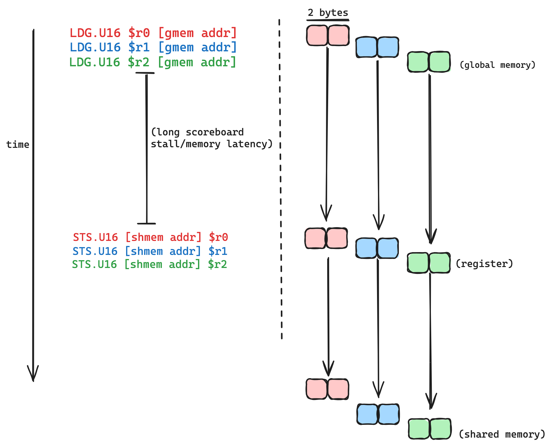 In the initial version, the total latency of the copy operation is roughly proportional to the memory latency of the device, times the number of loop iterations. After unrolling the loop, the total latency compared to the first version should be reduced by a factor of the number of loads the compiler decides to overlap with eachother (ish).
The other fairly easy optimization we can make here is to increase the number of bytes being loaded per instruction. Our load operation is currently compiling to LDG.U16, each of these instructions loads 16 bits/2 bytes from DRAM. The widest load instruction in SASS is LDG.128, which loads 128 bits/16 bytes. Since our kernel is bound by memory latency and not memory bandwidth, if we use a wider load instruction will experience the same latency per memory request, but move more bytes per request. We are amortizing the latency over more bytes moved, which is a win for efficiency.
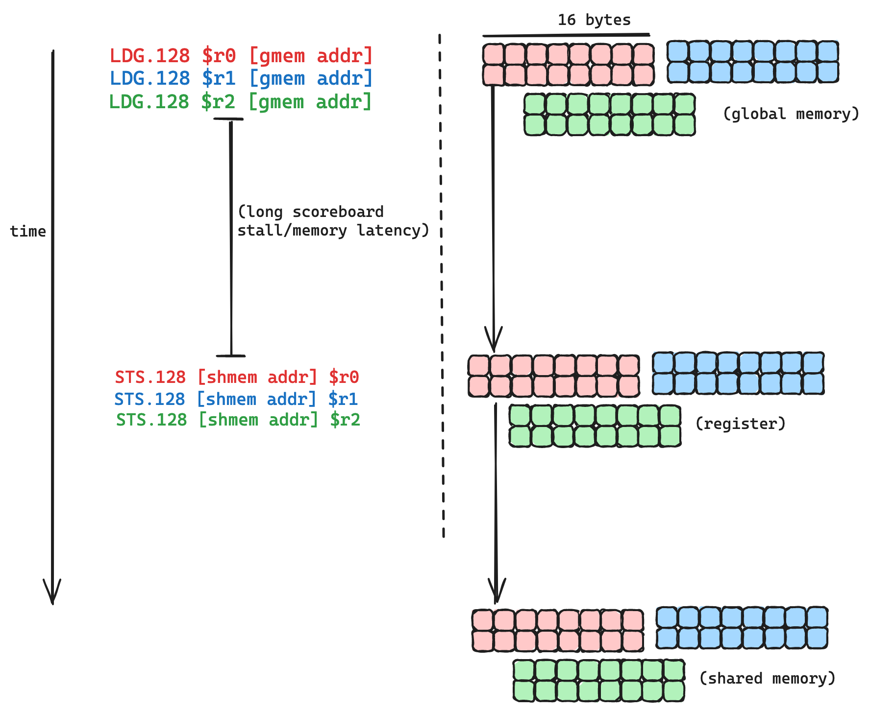
A quick and hacky way to accomplish this is by reinterpret_casting the src and dst pointers from half to float4, and updating the index and loop calculations accordingly. Here is a godbolt link to a kernel with the vectorized and unrolled memory copy, and here is the code.
These optimizations to the memcpy increase the throughput over the first kernel by about 3x. But there is still a long way to go before we approach cuBLAS level performance

Kernel 3 - Shared Memory Swizzling
Back to the warp state section of NSight Compute
 The long scoreboard stall is no longer the leading offender in terms of warp stalls, and our kernel got about 3x more performant after applying the optimizations described in the last section. Warps are now spending an average of ~19 cycles stalled per issued instruction due to something called “MIO Throttling.” What is MIO Throttling, and how do we address it? According to nsight compute docs this means:
Warp was stalled waiting for the MIO (memory input/output) instruction queue to be not full. This stall reason is high in cases of extreme utilization of the MIO pipelines, which include special math instructions, dynamic branches, as well as shared memory instructions.
In our case, this stalling is almost certainly due to shared memory instructions, since our kernel has very few dynamic branches, and no trigonometry or any other special math instructions. Specifically, it is due to shared memory bank conflicts. According to here two symptoms of shared memory bank conflicts are very high L1/TEX thoughput number (currently at 97% of peak) and MIO Throttle stalls, these are both second order effects of shared memory bank conflicts. I learned at this point that if you have a kernel whose performance is being killed due to shared memory bank conflicts, this is not blatantly obvious when you look at NSight Compute, however the information is definetly there. I found that in order to see where shared memory bank conflicts were occuring, and understand their severity, I had to learn the terminology of a “wavefront”. In order to understand this term, a bit of background on shared memory is required.
Background: Bank Conflicts and Wavefronts
From the perspective of a CUDA program, shared memory works as follows (here is the official guide). If you declare a __shared__ array in your kernel, it corresponds to physical memory that is located on a specific streaming multiprocessor. Consequently this array is fast to access, but only accessible by threads on the SM, which in the language of CUDA means that shared memory arrays are local to a particular thread block. Physically the memory is spread between 32 “banks” with each bank storing an adjacent 4 bytes, like so:
 Each bank can produce a single 4 byte value per clock cycle. If our goal is to maximize our reading and writing bandwidth from shared memory, we need to keep this in mind when deciding on an access pattern. Full bandwidth is achieved when the 32 threads in a warp spread their access uniformly across the 32 banks. Bank “conflicts” occur when a single bank must produce data for more than one thread for a given request. In order to show how the ideas of bank conflicts and wavefronts tie together, here are 3 scenarios, all in a simplified world where we have 4 threads and 4 memory banks
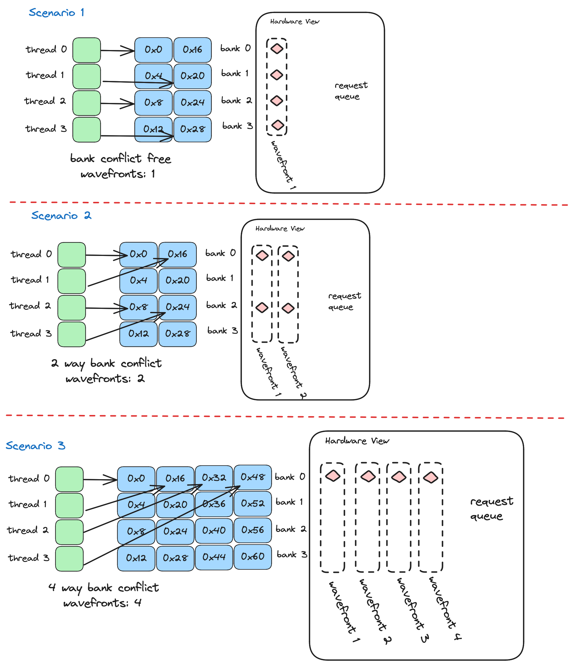 When loading or storing from shared memory, each thread requests a particular memory address that in our simplified world falls into one of the four memory banks. In scenario one, each thread is accessing data in a different bank, and the hardware calculates that these four accesses can be combined into a single transaction for the hardware to process, the word for this transaction is a wavefront. In scenario two, the four threads access addresses that fall into two of the four banks. Since each bank is only capable of sending one word at a time, the hardware groups these four requests into two wavefronts, and the memory hardware processes the two wavefronts one after the other. Scenario three is the worst case scenario, the four threads access addresses that all fall to the 0th memory bank, and in this case the four seperate wavefronts are required to service the transactions from the four threads.
For four threads accessing four bytes, the “ideal” number of wavefronts is one, because (ideally) regardless of which threads are accessing which bytes, we should be able to arange our data such that all of our accesses are spread nicely accross the banks. For example scenario three as shown is less than ideal, but we could make it ideal by transposing the bytes in shared memory, this would result in the four accesses falling evenly accross the four banks. But for the layout as shown, the actual number of wavefronts is four.
NSight Compute will tell us per memory access:
- the ideal number of wavefronts
- the actual number of wavefronts
- the number of wavefronts that are excessive, which is just 2 - 1
According to the analysis above, if our code has an $n$ way bank conflict, $n$ should be equal to $\frac{actual\ wavefronts}{ideal\ wavefronts}$. We want the actual to equal the ideal, this often requires some careful thinking about how data is being laid out and how threads are accessing it.
ldmatrix bank conflicts
Here is a screenshot of the per instruction actual/ideal wavefronts in NSight Compute:
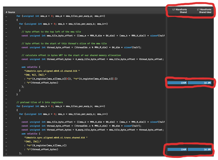 These
These ldmatrix commands are loading data from shared memory into thread local register memory in preparation for the MMA operations. NSight Compute tells us the ratio of actual to ideal is ~8ish, which suggests this memory access results in an 8-way bank conflict. In order to form a strategy for fixing this performance killer, we need to understand why it is happening.
In the tiling structure shown for Kernel 1, in each iteration of the warp loop (the green one), a single warp is responsible for reading a 64x64 tile of data from shared memory, and writing it to registers. The shared memory reads are where the bank conflicts occur. In the visualization below, on the top is a very zoomed out version of one of these 64x64 tiles, the layout across memory banks is visualized by the color of the columns. We can see that a row of 64 elements, which are 2 bytes each, nicely spans the 32 memory banks.
On the bottom is a zoomed in version of a single 8x8 tile that is brought from shared memory into registers by ldmatrix. Each warp is iterating over its own local 64x64 tile in 8x8 increments, calling ldmatrix on each little tile, this PTX instruction loads values from shared memory, and shuffles the loaded data among the registers in a warp to match the register layout that the tensor core instruction expects.
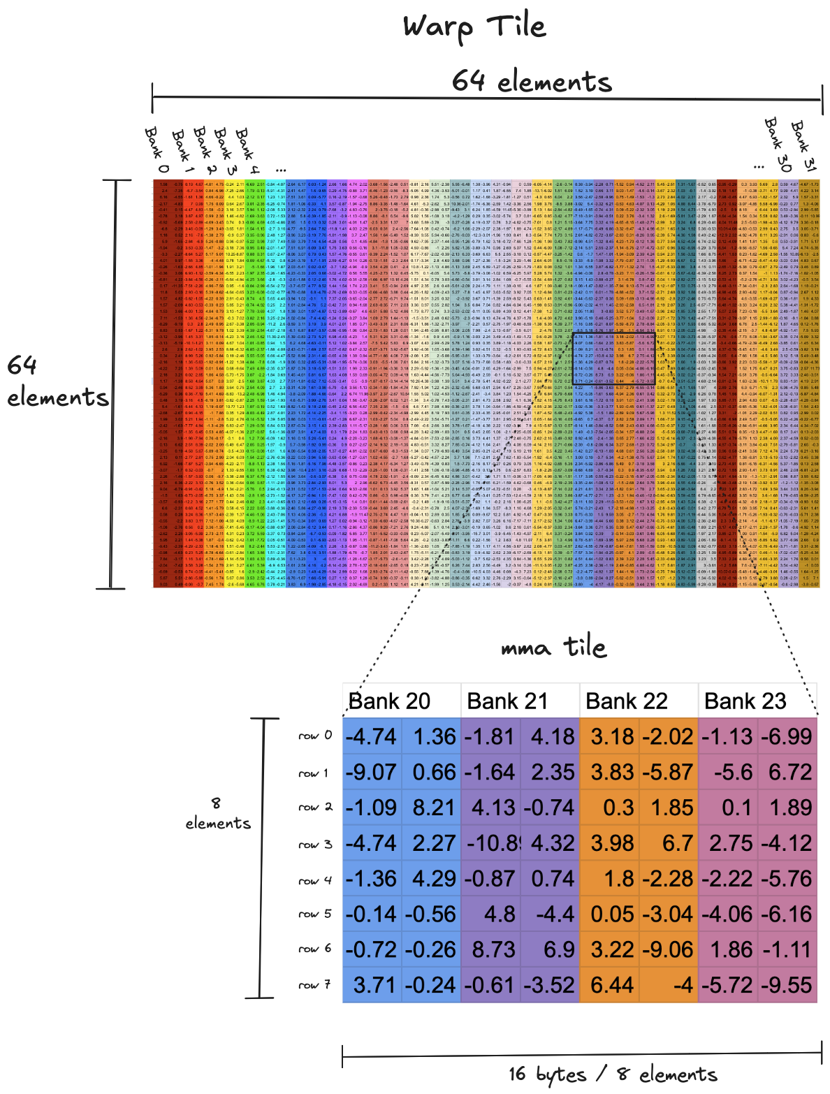 The inner workings of
 ldmatrix are a bit opaque, it compiles to a single SASS instruction LDSM..., rather than multiple explicit shared memory loads and register shuffles, as one might expect. However, we dont need an understanding of ldmatrixs inner workings to see why the 8 way bank conflict is occuring each time we call it. Rather the 8-way bank conflict is an inevitable result of the fact that each row in a given tile is spread across the same four memory banks. One wavefront is required to read each row, and there are eight rows, which means eight wavefronts. Ideally, if the eight rows in each tile were spread evenly across the thirty two memory banks, the entire tile could be read with a single wavefront. Reading these tiles is in the inner loop of the kernel, for $8192$x$8192$ operands we read a total of $ (8192/8)^3=1,073,741,824$ of these tiles which works out to a ~shitload~ of bank conflicts. So if we care about performance, it is worth the time to fix it.
Padding
In order to have a bank conflict free kernel, we need to rearrange the layout of data in shared memory such that we can read and write to shared memory without any excessive wavefronts. The challenge comes from the fact that the thread to data mapping for shared memory reads is different from that of shared memory writes. When writing, adjacent threads write adjacent values in a row, whereas when reading adjacent threads read adjacent values down a column.
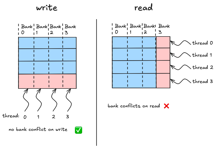
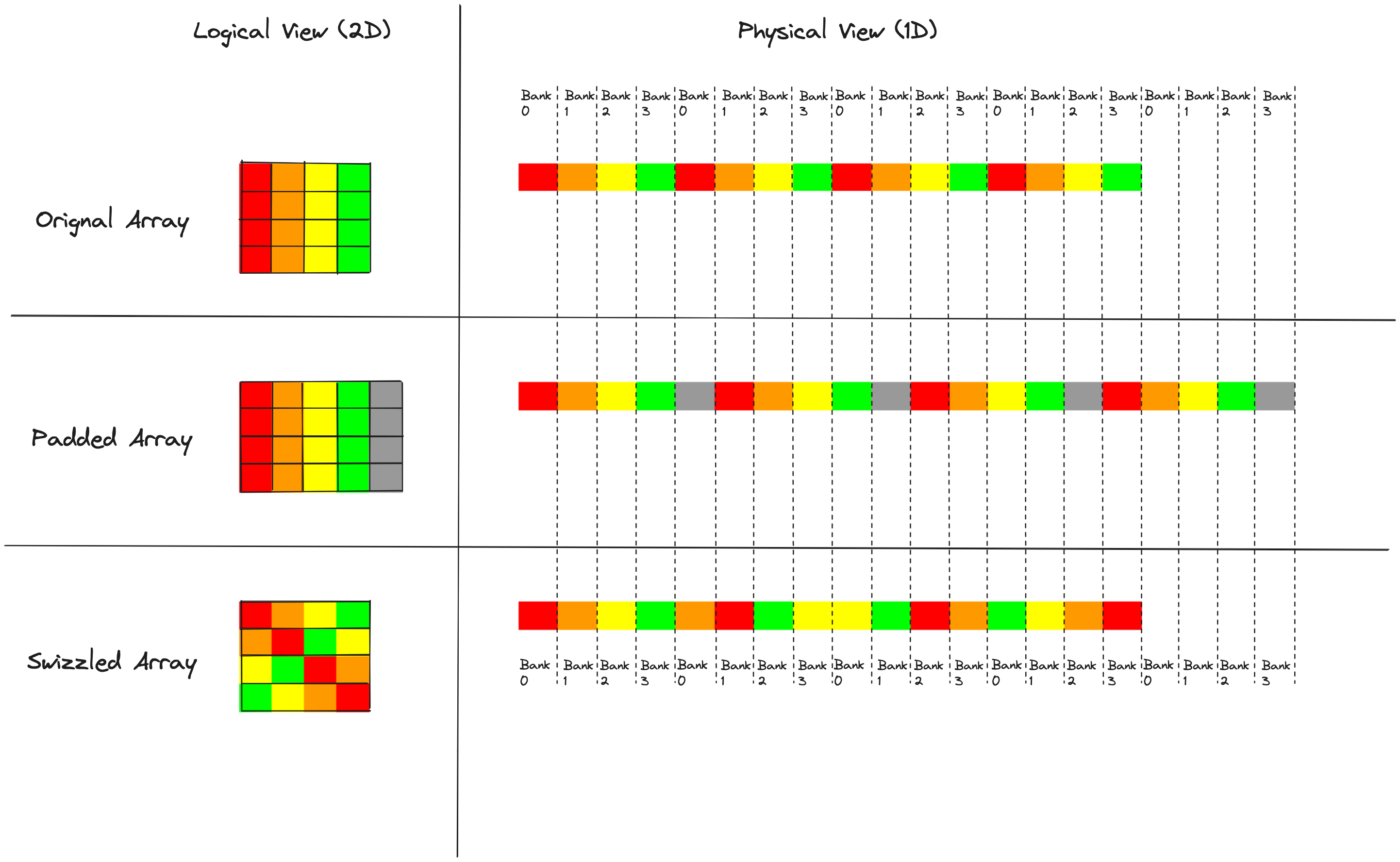
This is a common situation in kernels that use 2d shared memory tiles, and the standard fix is to add a bit of padding (i.e. empty space) at the end of each row in the shared memory array. If we add this padding in such a way that a single row of our array no longer fits perfectly into the 32 memory banks, adjacent values in a column no longer fall into the same bank, which means we can read columns with no excessive wavefronts. This makes more sense in a picture than in words, here again is a simplified case of a mini-array (4 columns and 4 rows) stored on a mini-gpu with only 4 memory banks:
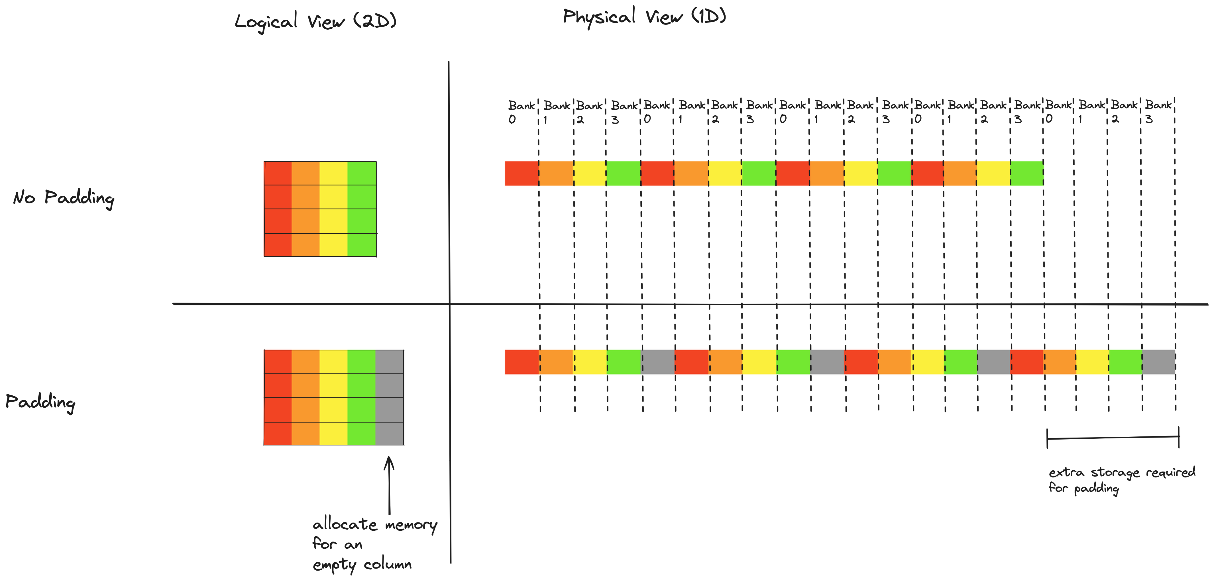 Array elements are color coded by column. Notice that in the no padding case, all the array elements in a given column fall into the same memory bank. After adding the column of padding, the array elements in a given column are spread across all 4 memory banks. The padding technique could be used here to fully eliminate bank conflicts. Since we are using vectorized writes to shared memory, we are writing to shared memory in 16 byte chunks at a time, and each chunk must be aligned. Adding 16 bytes of padding to each row of shared memory would result in each 8x8 mma tile being spread across all 32 memory banks (exercise of convincing yourself of this left to reader).
The drawback of using the padding technique is that it requires us to allocate extra, unused space in shared memory. In Kernel 2, the shared memory tile for $A$ is 256x64, and the shared memory tile for $B$ is 128x64. If we add an extra 16 byte, or 8 element column to both of these, that will increase the amount of shared memory we allocate by 25%, for a total of increase of 6144 bytes. This wasted space turns out to be a significant drawback, when writing a high performance kernel shared memory is very precious stuff - this becomes especially apparent later down in the road when using a technique called double buffering, each threadblock in future kernels will end up using 100% of the 65536 bytes of shared memory on each SM. So, we should wonder whether there is a way to eliminate bank conflicts without wasting any shared memory space. It turns out this is very possible!
Swizzling (toy example)
Swizzling is probably my favorite technique that I learned in the process of working on this. The word “swizzle” has several different uses, when used in the context of cocktails it means to stir and when used in the context of GPUs it means to rearrange. In our context of eliminating shared memory bank conflicts in 2D tiles of data, swizzling means permuting the elements within a tile of shared memory such that we can access the data without any bank conflicts. This is one of those techniques that seemed like black magic to me until I took the time to understand it, and now I appreciate its cleverness and elegance.
In our 4x4 tile, we add the padding because it shifts the alignment between data and memory banks in a desirable way. Swizzling is based on the observation that we don’t need the extra padding bytes to spread column elements evenly over memory banks. Instead we can just figure out a permutation of matrix elements that spreads around the columns in the right way, and apply this permutation when we write to shared memory. Here is an illustration of a “swizzle” i.e. a permutation of elements that can eliminate bank conflicts.
 It is worth remembering at this point that our shared memory layout must satisfy two requirements, bank conflict free row access for writing, and bank conflict free column access for reading.
In all three cases, each row is consecutive in memory and spread across all four memory banks, which means each row can be written without any bank conflicts. The observation here is that when we apply our permutation or “swizzle”, we don’t want to permute elements across rows, only within rows; otherwise we might lose this property of bank conflict free writes.
The problem that motivated us to think about shared memory layouts was the bank conflicts that occur when we read columns. Adding the padding fixes the bank conflicts here, but at the expense of wasted shared memory. Swizzling gives us the best of both worlds; we can read columns with no bank conflicts, and no shared memory is wasted. So how do we think about applying this permutation?
The swizzle shown above can be implemented as a function f that maps indices to new indices. If A is the original array, A_s is the swizzled array, and i is the index of an element, then A_s[f(i)] = A[i]. So what is f here?
Since f is operating on array indices, we should think about the different ways these indices can be represented and viewed:
 On the far left are the 2D row and column indices. Moving to the middle, these indices can be linearized into a sequential (and in this case row major) ordering of the 16 elements in the array. Moving to the right, when we look at the sequential indices in binary we can see that the 2d structure is present in the index bits. The two least significant bits in the index encode the column and the two other bits encode the row. As a spoiler alert,
 f is going to operate from the perspective of the view on the right, the binary representation of the flat array index. Here are two observations about what f needs to do:
- In order to avoid bank conflicts on write, we want to permute elements within a row, or in other words no elements should switch row. This means that
fshould modify the bits which encode the column, and leave alone the bits that encode the row. - We want to apply a different permutation to each row, and for any given column, we want the elements in that column to be spread across all four columns in the swizzled array.
We can accomplish both of these aims using the XOR function, specifically by XORing the row bits of each element with its column bits, and using the result as the new row bits. Here is a row by row break down that shows how XORing the column bits with the row bits moves around values within a row:
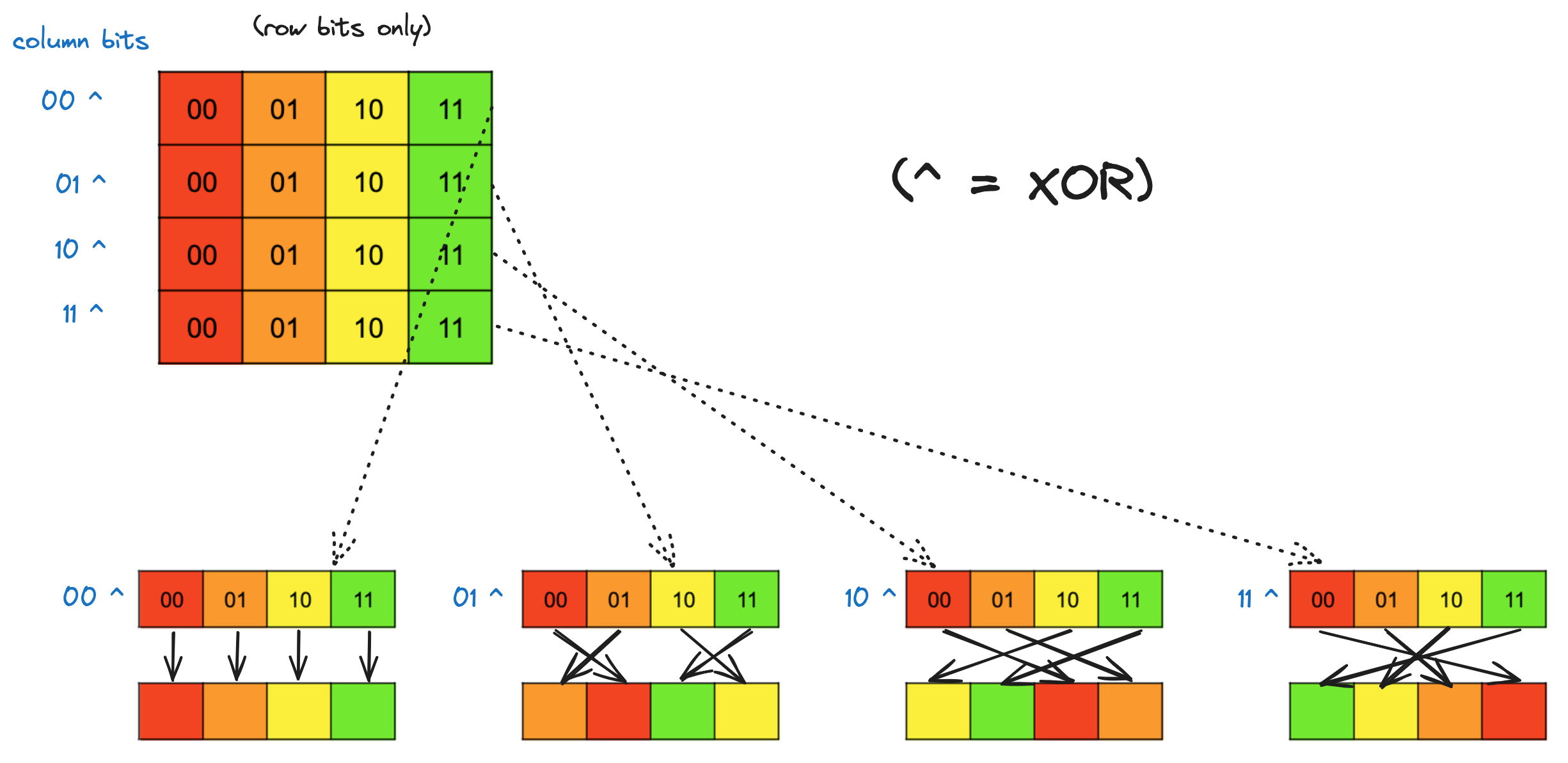 The
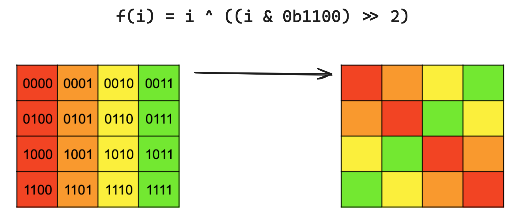
The f that does this for us is f(i) = i ^ ((i & 0b1100) >> 2). The mask is selecting the two column bits from i, these two bits are then shifted right two places so that they line up with the two row bits for i, and then we XOR. i’s column bits remain unchanged.
Here is a visualization of the result of applying this function for all rows together:
Swizzling (real world)
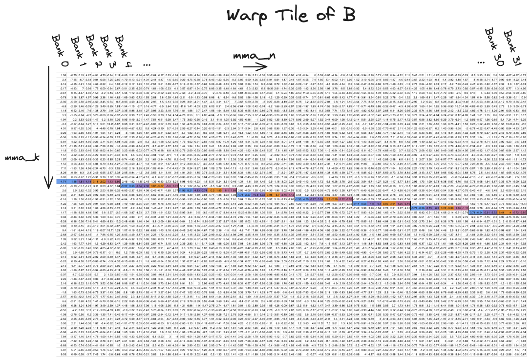
Now we need to figure out how to use this technique to permute our shared memory layout in such a way that we can read a single 8x8 mma tile with 0 excessive wavefronts. As a reminder, here is a view of our shared memory layout, with a single tile of interest highlighted.
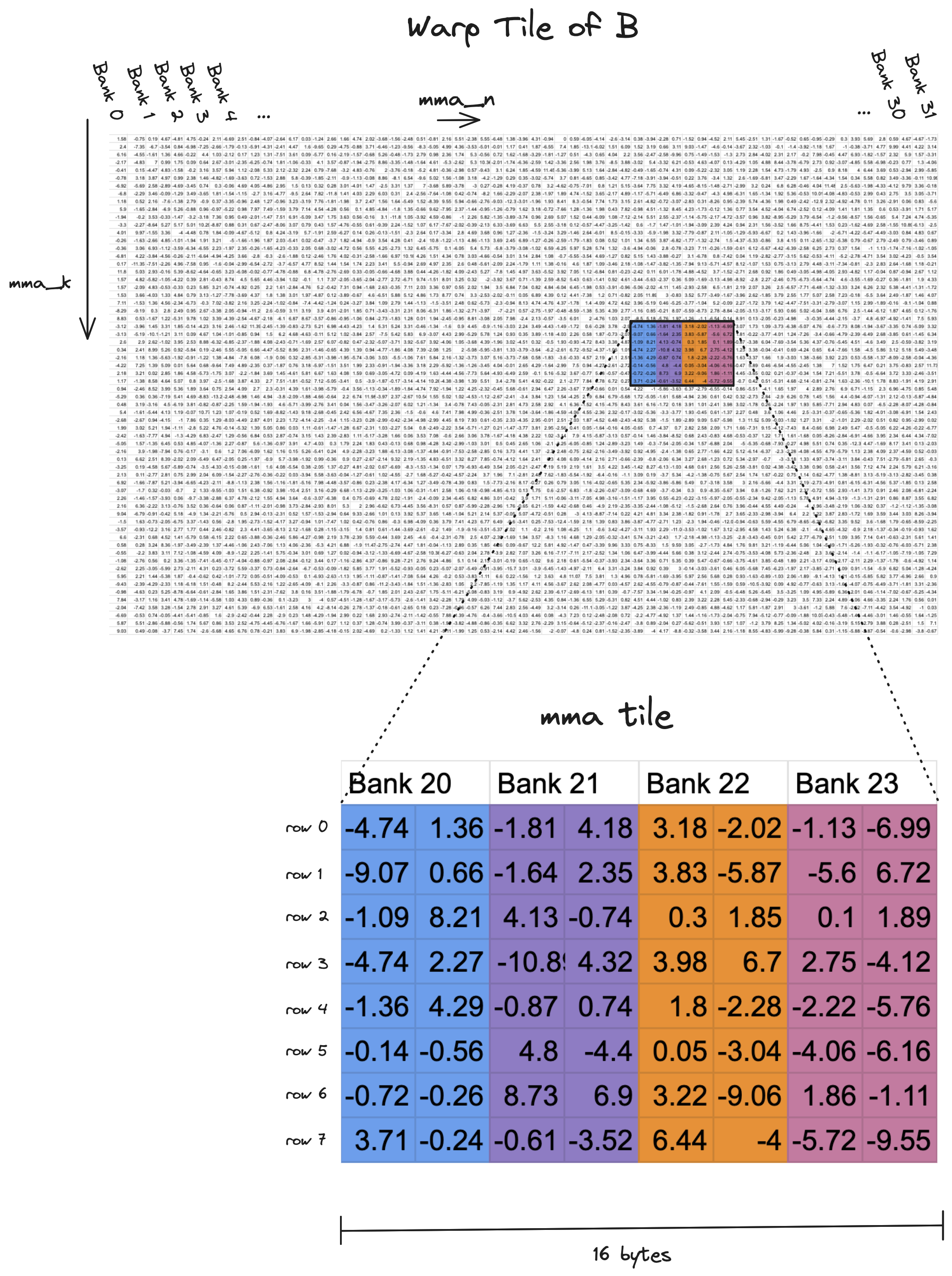
Our goal is to figure out a swizzle function that spreads the 8 rows in this tile across all 32 memory banks, rather than having all 8 rows stuffed into 4 memory banks which is the case above. From the view of the full tile, the rows of the tile above would be spread like this.
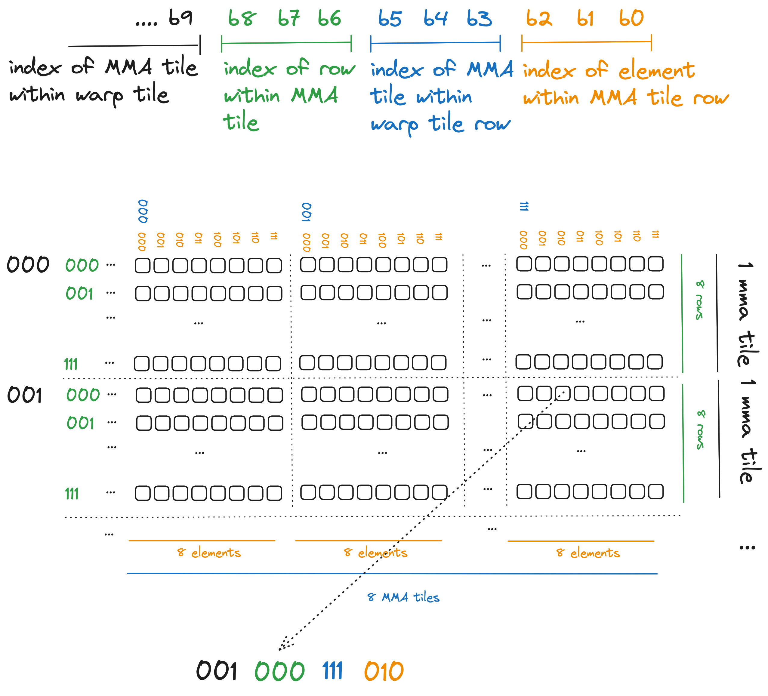
In order to figure out what swizzle function we should use, lets look at the binary representation of an index into this tile, and assign it some structure that corresponds to our tiling scheme.
Some notes about what our swizzling function should do and not do:
- We want to keep the eight elements in each MMA tile row together. In other words, eight adjacent elements in a single row of an 8x8 MMA tile are going to stay together when we apply the swizzle. This means our swizzle function is not going to touch the orange bits.
- Bank conflicts occur because the 8 rows within an MMA tile are all perfectly stacked on top of each other. Within an MMA tile, we want to spread these 8 rows horizontally across the entire warp tile. The blue bits encode where in the 64 element wide warp tile each MMA tile falls, so these blue bits are the ones we want our swizzle function to modify.
- We dont want to move elements between rows, so our swizzle function is not going to modify the green row bits. However, these green row bits provide a nice alternating pattern that we can XOR with the blue bits to mix around the MMA tiles within their row.
- Again, we dont want to be moving elements between rows, and the black bits (the most significant ones shown in this diagram) encode the starting row of each MMA tile. Our swizzle function is going to ignore them.
So what this all means is that for each index, we want to take the blue bits, XOR them with the green bits, and replace the original blue bits with the result of this XOR. If i is the index we want to swizzle, this works out to:
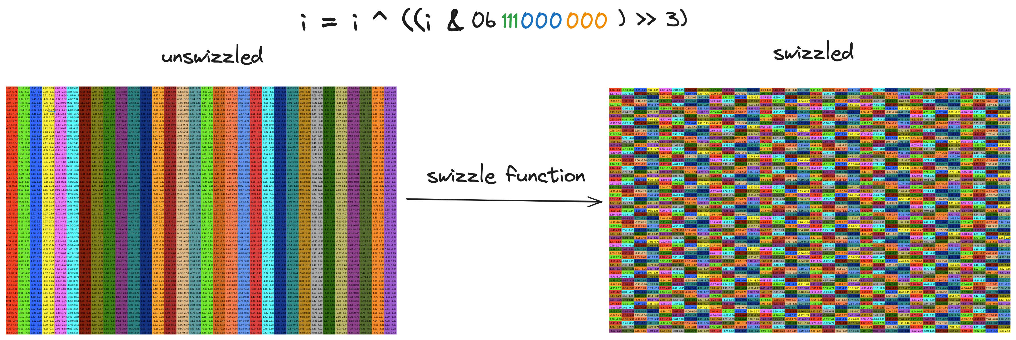 And just like that, we have no bank conflicts. Swizzling takes a bit more figuring out than the padding technique, the choice of swizzle function depends on the shared memory array dimensions, and the vector width we are using for reads/writes (i.e.
 float4, float2, int, e.t.c.). As a result, if we use swizzling it adds an extra consideration each time we consider changing either of these. But if you want to eliminate bank conflicts and dont want to increase your shared memory footprint in the process, swizzling becomes necessary. I think it is very elegant and clever, if you compare kernel 2 with kernel 3, there is a total of ~4 lines of code that change, these four lines are the addition of the swizzle into the shared memory index calculation.
I figured all this out by looking at the Swizzle class implemented here in the CUTLASS repository. Via its three parameters, bits, base, and shift, this class represents a family of swizzle functions that shift and XOR bits of array indices. I have also seen examples of more exotic swizzle functions (see slide 27 here) that go beyond what is representable by the implementation in CUTLASS. I found it helpful to visualize the permutations applied by different swizzle functions, to help with this I wrote a bit of python code that pretty-prints arrays, applies swizzle functions, and counts bank conflicts.
Eliminating bank conflicts results in a ~2x speedup, and gets us to about 50% of the cuBLAS level thoughput.
Kernel 4 - Makeshift Async Copy
Each optimization addresses the least performant part of the previoius kernel. After applying each optimization, if it worked, the least performant part of the kernel should change. Before fixing the shared memory bank conflicts, the shared memory operations inside the inner loop were the bottleneck. After eliminating bank conflicts, the inner loop becomes much more efficient, and the bottleneck is once again the latency of the global memory to shared memory transfer. This was addressed with vectorizing and loop unrolling in Kernel 2, but after fixing bank conflicts, NSight Compute is telling us that there is more latency here to hide. Here is pseudocode of the current loop nests, with a zoomed in view of the code that needs to be improved:
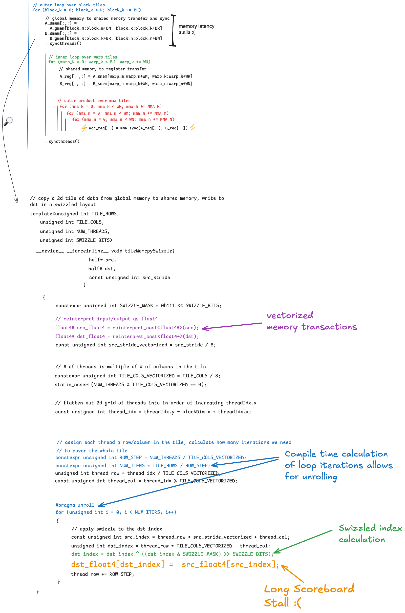 Once again the issue is that the line which performs the global memory to shared memory copy:
dst_float4[dst_index] = src_float4[src_index];
// shared memory        // global memory
This^ is a blocking operation from the perspective of hardware, in the sense that when a given thread executes the resulting assembly the thread will be stalled for the full duration of to data arriving from global memory. The above line is equivalent to this:
float4 tmp = src_float4[src_index]; // global memory to register
dst_float4[dst_index] =  tmp; // register to shared memory
The global memory to register transfer, which is the first line, incurs latency because data is coming from off chip. When it comes time to store from register to shared memory (second line) the hardware detects that the data needed from global memory has not yet arrived in tmp, and execution stalls until it arrives. In Kernel 2 we addressed this performance issue by amortizing the latency over more data moved per transaction (vectorizing) and helping the compiler to interleave multiple loads/stores, which hides latency (loop unrolling). But NSight Compute tells us that even after these optimizations, this sort of stall, on this line specifically, accounts for about ~20% of the total clock cycles that the kernel spends stalled.
The key observation here is that if we break down the dst[...] = src[...] line into its two constituent parts, we can break them apart so that other useful work is being done while the data is in flight from global memory.
The general idea is that we can prefetch data from global memory into register storage, one block_k ahead of the block_k we are currently computing on. At a very high level we want to go from this:
float4 tmp = src_float4[src_index]; // global memory to register
// (stall while we wait for data to arrive from memory)
dst_float4[dst_index] =  tmp; // register to shared memory
{
    // compute inner loop for current block tile
}
to this:
float4 tmp = src_float4[src_index]; // global memory to register
{
    // compute inner loop for previous block tile
}
dst_float4[dst_index] =  tmp; // register to shared memory
The key improvement being made here is that we are initiating the load of data from global memory corresponding to block_k, and performing the compute corresponding to block_k-1 concurrently. In doing so we are hiding the latency of loading the block_k tiles of $A$ and $B$ with the computation corresponding to the block_k-1 tiles.
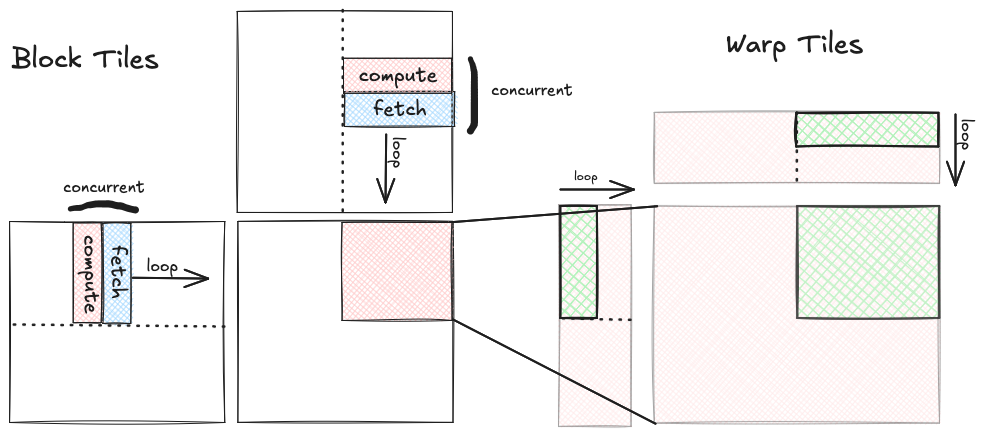
This improved overlapping of data movement and compute is accomplished by
- adding new register storage to hold the data that is prefetched from global memory
- breaking up the global to shared memory transfer into its two components, putting these two components on opposite sides of the inner loop (over warp tiles and mma tiles)
- and tweaking the position of the two
__syncthreads()in the outer loop to allow for the concurrency we want, while still preventing race conditions.
Here is before/after pseudocode which shows how the data movement changes.
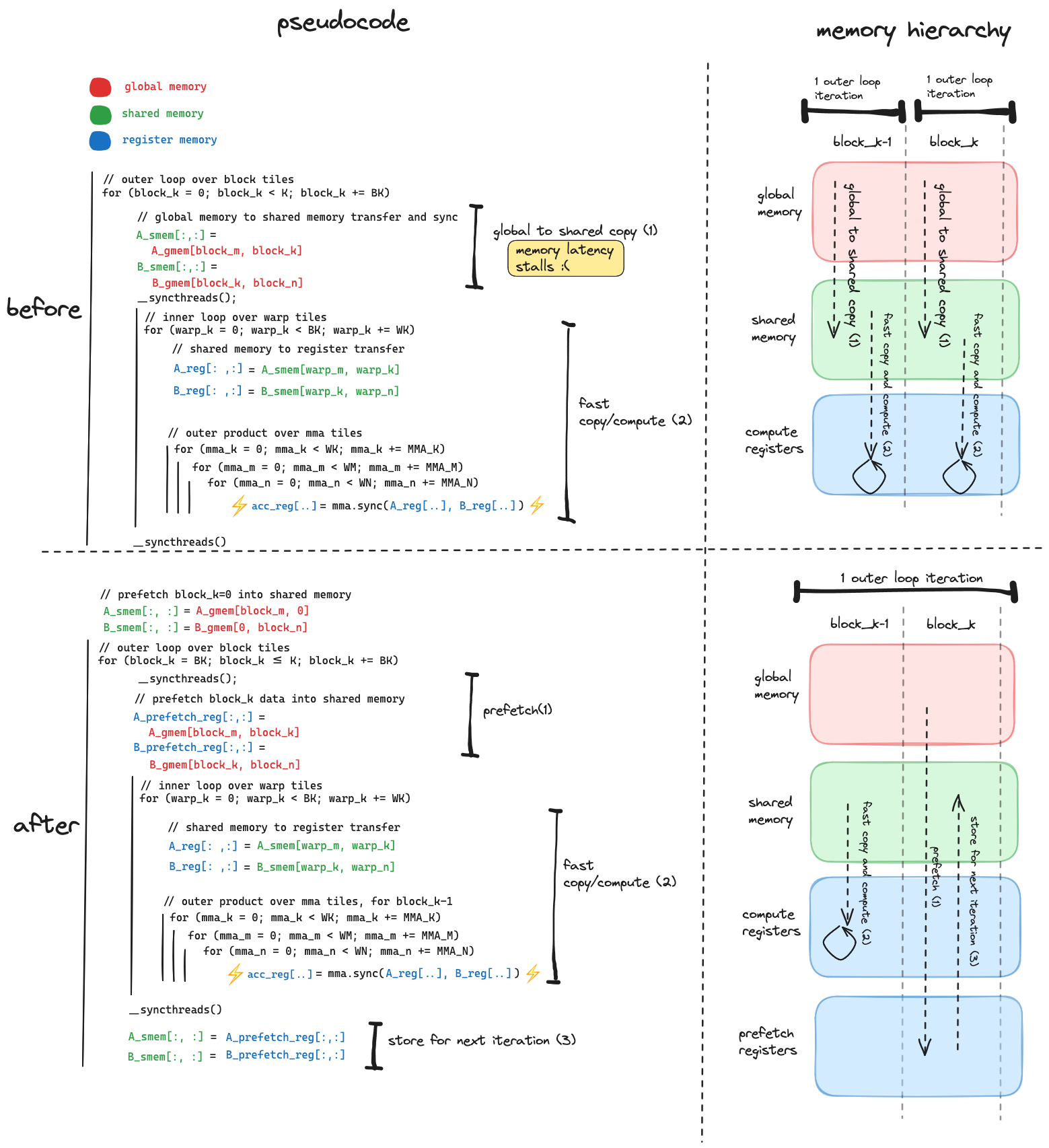
This produces a nice speedup over the previous kernel, and gets us to ~70% of the HGEMM kernel.
GPU occupancy (digression)
The potential cost of this optimization is that it requires additional register storage, each thread block stores two additional block tiles worth of data in register memory. According to the Launch Statistics section in NSight Compute, we go from using 104 registers per thread in Kernel 3, to 166 registers per thread in Kernel 4. This increase resource usage per thread has the potential to hurt kernel performance because it can impact how many threads the hardware is capable of executing concurrently. This is a quick digression on why increasing register use per thread has the potential to hurt performance, but why in this case, it doesn’t.
This gets to a topic called occupancy which is central to the CUDA hardware and software implementation. Each streaming multiprocessor (SM) will maintain block, warp, and thread execution state (shared memory, registers, program counter) on chip, for as many thread blocks as can be fit. The amount of thread blocks that can be fit on an SM depends on:
- how much shared memory, registers per thread, and number of threads each thread block needs to execute (this a property of a given kernel, and the launch configuration of that kernel)
- how much shared memory, registers per thread, and number of threads the SM can handle at once (this is a property the device, and improves from generation to genereation)
If a given kernel implementation and launch configuration require only a small number of registers, a few threads, and a small amount of shared memory per block, an SM can execute lots of thread blocks concurrently. When multiple thread blocks are executing concurrently on an SM, context switching between them is free. This allows the hardware to hide stalls and latency simply by tracking which threads are capable of executing their next instruction and which are not, and issuing instructions for whichever threads are ready. The more threads the SM has to choose from, the better this works. This is called hardware multithreading, and lots of older resources on CUDA performance talk about it as the primary guiding principle for writing fast kernels.
At this point, the limiting factor on the number of thread blocks that can be resident on an SM is shared memory. Each thread block is allocating a $(256,64)$ tile of shared memory for for the $A$ matrix, and a $(64,128)$ tile of shared memory for the $B$ matrix. This works out to 49KB of the total of 62KB of shared memory per SM, which limits the number of thread blocks that can be resident on an SM to one at a time. So in this instance, since shared memory is the limiting factor, using more registers per thread doesn’t matter.
The high performance GEMM kernels typically have lower occupancy, meaning they use more shared memory and register memory per thread, and have less threads resident on an SM at once. This is primarily because of the need for high arithmetic intensity; in order to keep compute units busy with limited memory bandwidth, the more compute per thread at low levels of the memory hierarchy, the better. But the drawback of low occupancy is that the GPU will be less effective at automatic latency hiding via context switching. We can deal with this tradeoff by structuring our kernel to allow overlap between compute and data movement, this chapter is an example of this.
The two newest NVIDIA architectures, Ampere and especially Hopper, introduce dedicated hardware suppport that allows us to perform several components of GEMM kernels asychronously (more on this in conclusion). This hardware support makes writing efficient, low occupancy kernels such as these ones much easier.
Kernel 5 - Tune Tile Dimensions
Up until this point, I found that after 10 minutes or so of looking at profiling results in NSight Compute, I would know exactly where the bottleneck in the kernel was, and what was causing it. After Kernel 4, which achieves about 70% of the cuBLAS thoughput, the profiler generally would not point to a single performance issue. In hindsight this was because the remaining 30% between kernel 4 and cuBLAS is the product of many smaller inneficiences, as opposed to one single one, and performance optimization began to have more of a trial and error flavor based on hunches, some of which turned out to be wrong. This chapter contains a description of two optimizations, that when implemented together produced a decent speedup.
tune tile dimensions
At this point I began to wonder, if my kernel were still memory bound, how would I know? If you are using single precision FFMA instructions the “Speed of Light” section in NSight Compute will show you a roofline chart, but not if you are using tensor cores. I was inspired by this paper to try to figure it out myself in a back of the envelope sort of way.
A more actionable way to formulate the “am I memory bound?” question is “does the arithmetic intensity of my kernel exceed the machine’s balance point?”
\[\frac{FLOPs\ performed}{bytes\ moved} \stackrel{?}{>} \frac{\tau}{\beta}\]So for the left hand side, we need to substitute in numbers that are specific to our kernel, and for the right hand side we need to subsitute numbers specific to our hardware. This section went over how arithmetic intensity is a function of tile sizes. Namely for tile dimensions $BM,BN$ and $BK$, the arithmetic intensity we should expect is $\frac{BM * BN}{BM+BN}$. Here is a refresher of this, specific to the block tile level
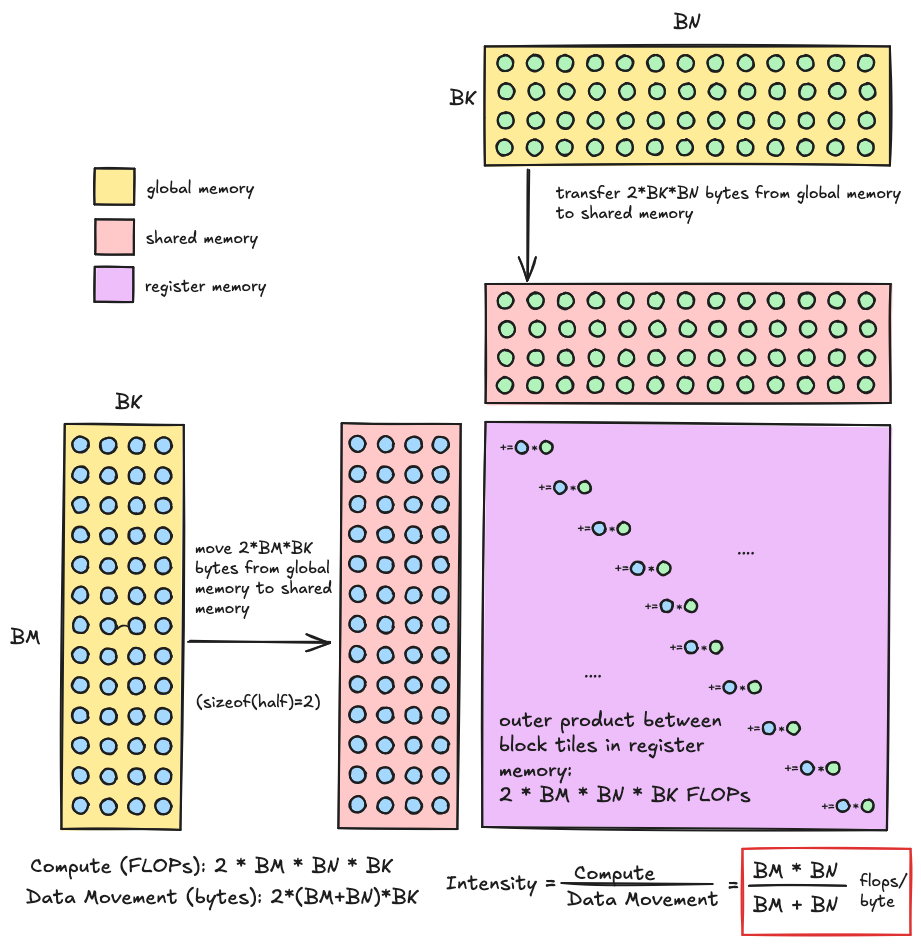 Notice how $BK$ cancels out in this calculation. This means when thinking about arithmetic intensity, the size of our tiles along the $K$ dimension are irrelavent. However, when thinking about other aspects of performance it is not irrelavent (more on this later).
M and N Dimensions / L2 cache locality
We now need to subsitute in numbers for our machine balance. Earlier in the roofline charts we set $\tau_{HMMA}$ to the throughput of the cuBLAS hgemm kernel, which likely errs on the side of being an underestimate. In this case, the goal is to choose tile dimensions that are large enough to put us comfortably in the compute bound regime of the roofline chart, so I would like to instead err on the side of overestimating the arithmetic throughput in the numerator of the machine balance, and err on the side of underestimating the memory bandwidth in the denominator.
A reasonable overestimate of $\tau_{HMMA}$ is 65,000 GFLOP/sec, which is the theoretical peak found on the T4 data sheet.
When it comes to the memory bandwidth in the denominator, we want to conservatively estimate our achieved memory bandwidth. In order to do this, we need to consider the effect of the L2 cache. The L2 cache is shared between the 40 streaming multiprocessors on the T4. In practice this means that when one thread block accesses data from DRAM, it is moved into the L2 cache, and accesses to the same data originating from other thread blocks will hit the L2 cache, until this piece of data is evicted.
According to people on the internet, thread blocks execute in increasing order of their flattened block index. The official CUDA programming guide says that different thread blocks execute independently, and the programmer should not assume any relationship between different thread blocks. So relying on this assumption for correctness would probably be unwise, but for a quick and approximate calculation on L2 cache locality it is helpful.
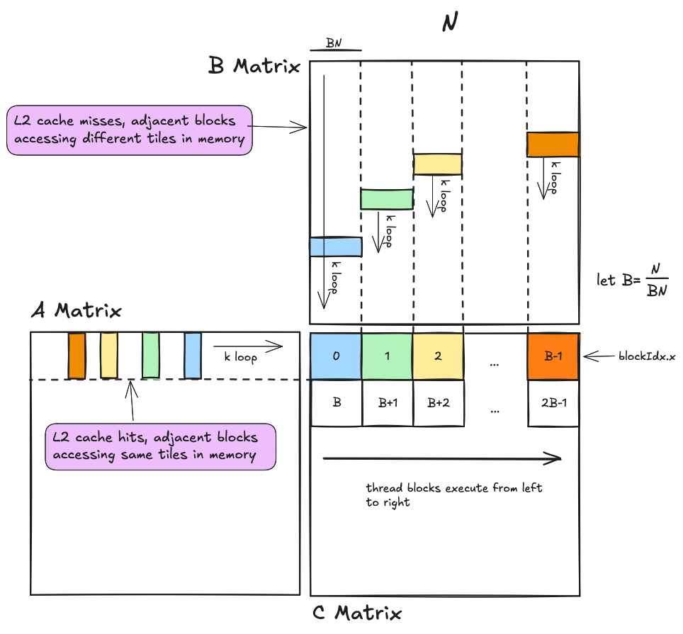 The basic idea here is that he accesses to the $A$ matrix from thread blocks executing at the same time have much better locality than accesses to the $B$ matrix. Most of the access to $A$ should hit the L2 cache, whereas most of the accesses to $B$ should miss, which means we should achieve roughly a 50% hit rate for global memory accesses. This means our achieved memory bandwidth is a 50/50 weighted sum between the DRAM bandwidth and our L2 cache bandwidth. Substituting this weighted sum in the denominator of the expression for machine balance finally gives us:
Plugging the current block tile dimensions ($BM=256$ and $BN=128$), memory bandwidths, and theoretical arithmetic throughputs gives us
\[\frac{256 * 128\ FLOPs}{256 + 128\ bytes} \stackrel{?}{>} \frac{65,000 * 10^9\ FLOPs/sec}{0.5 * 220 * 10^9 + 0.5 * 1280 * 10^9\ bytes/sec}\]which works out to an arithmetic intensity of $85.3 \frac{FLOPs}{byte}$ and a machine balance of $87.24 \frac{FLOPs}{byte}$. The fact that these two numbers are very close suggests that global memory access may still be dominating our overall runtime. If we can spare the space in shared memory, increasing our $BN$ dimension from 128 to 256 might be worthwhile. If $BM$ and $BN$ are both 256, our estimated arithmetic intensity becomes $128.0 \frac{FLOPs}{byte}$, which should hopefully put us comfortablly in the compute bound regime.
When considering the next level down in the hierarchy, the high shared memory bandwidth gives us a bit more wiggle room. Our swizzled shared memory layouts should result in bank conflict free access, giving us the full bandwidth of 3662 GB/sec. The $WM$ and $WN$ dimensions of the warp tiles are both 64. Plugging numbers into here:
\[\frac{WM * WN}{WM+WN} \stackrel{?}{>} \frac{\tau_{HMMA}}{\beta_{shmem}}\]gives an arithmetic intensity of $32 \frac{FLOP}{byte}$ and a balance point of $17.7 \frac{FLOP}{byte}$. Thus it is safe to assume that shared memory loads are not the dominant factor in our kernel’s runtime. However, in order to err on the size of more arithmetic intensity I also ended up increasing $WM$ and $WN$ while making $WK$ smaller.
K Dimension
Different considerations come into play when considering our tile sizes along the K dimension. In our pencil and paper analysis, the tile size along the K dimension cancels out of the expression for arithmetic intensity. When thinking about tile lengths along this dimension, different considerations come into play. First, we can use it to adjust the total size of our tiles without affecting arithmetic intensity. In the case of block tiles, the total amount of bytes of shared memory they consume is $BK* (BM+ BN)* sizeof(half)$, thus increasing $BK$ by a unit increases the total size of the block tiles by $(BM+ BN)* sizeof(half)$. In deciding the length of the block tiles along the K dimension, this becomes the primary consideration. With $BN=256,BM=256$ we choose $BK=32$, with these dimensions the total amount of shared memory used by tiles of $A$ and $B$ works out to 32KiB, which is exactly half of the shared memory per streaming multiprocessor. This decision makes sense in the next section, which discusses a technique called shared memory double buffering. This optimization involves allocating two buffers in shared memory corresponding to each input matrix, so one can be written to while the other is being read. When double buffering is implemented, with these tile dimensions we will be using every available byte of shared memory on the device.
tile dimensions - longer and thinner
Here is a visualization of the before/after:
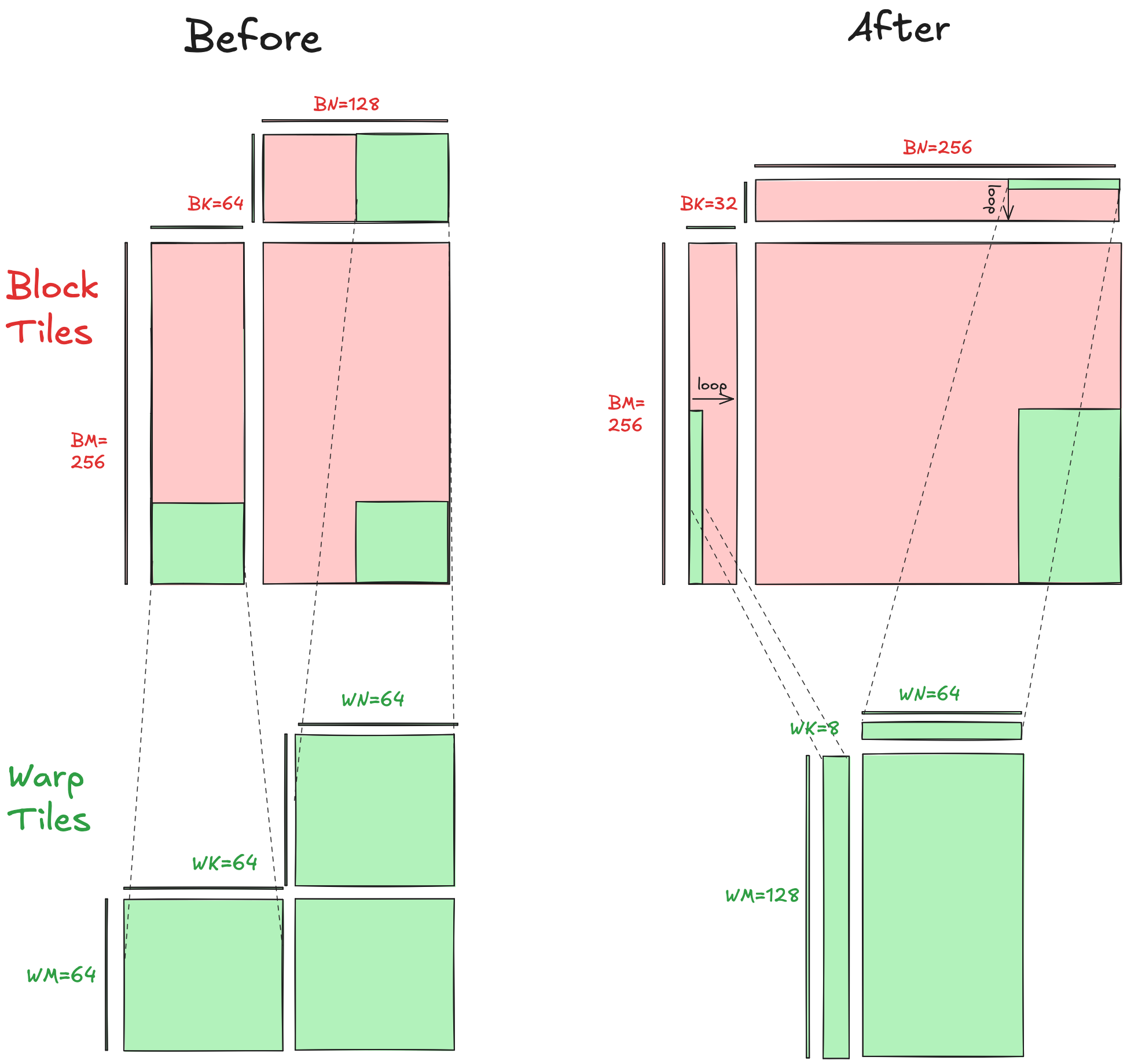 Both block tiles and warp tiles are made longer, and narrower along the K dimension, in order to increase arithmetic intensity. For the sake of time I combined this optimizations with the optimizations discussed below, so I did not measure the performance improvmement of this in isolation.
Kernel 5 - Optimize Index Calculation
At this point I was at about 70% of cuBLAS performance, my main strategy for using NSight Compute was to compare kernel metrics between my kernels and the cuBLAS HGEMM kernel. While the source code of the cuBLAS HGEMM implementation is not released by NVIDIA, looking at its metrics collected by NSight Compute can give us some insights into the sorts of optimization techniques that the clever folks at NVIDIA might have used when writing it.
The one thing that jumped out at me was that the total number of executed instructions of cuBLAS HGEMM was $94,175,232$, whereas Kernel 4 was executing $216,227,840$, over twice as many instructions as compared to Kernel 4. While Kernel 4 partly compensates for this by having a lower cycles per instruction ratio (8ish, vs 12ish for cuBLAS), this is certainly worth looking into.
So I wondered, why is my kernel executing twice as many instructions? Expanding the instruction mix section in NSight Compute gives us more information.
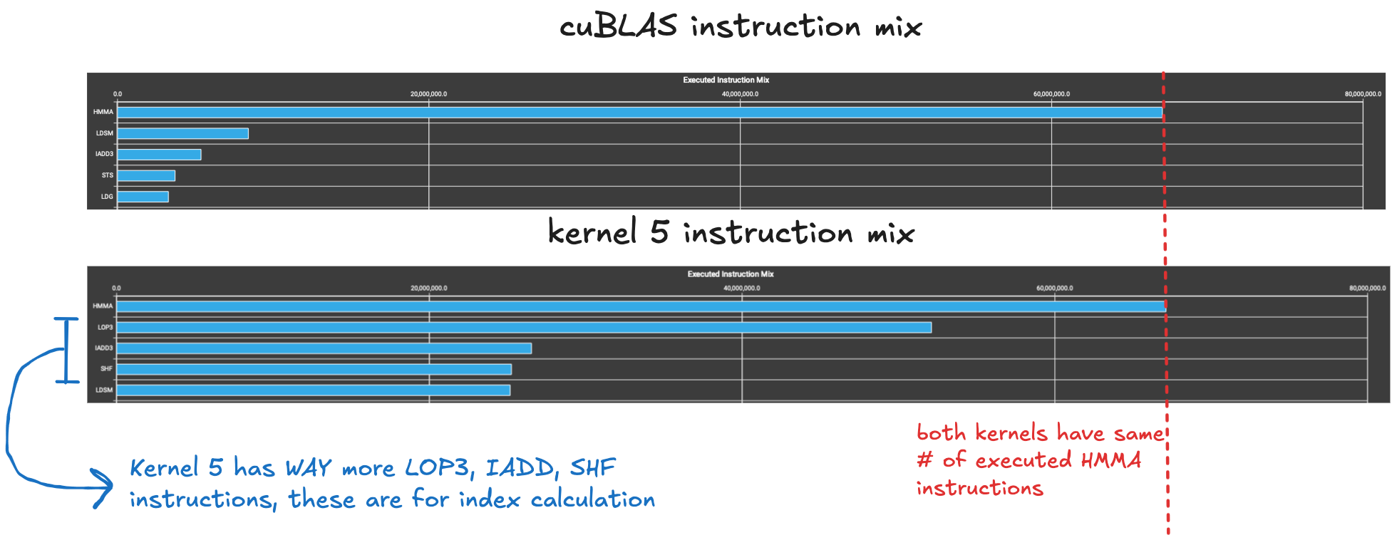 The answer is that Kernel 4 is performing way more index calcuation related instructions than the cuBLAS kernel. The
 LOP, IADD3, and SHF instructions are integer and logical instructions, these are different pipelines from the tensor core and can execute concurrently with floating point math happening elsewhere on the chip. However, each warp scheduler on a streaming multiprocessor can only issue a single instruction per cycle, and so the large number of index calculation instructions is likely crowding out the issuing of the HMMA instructions, these are the tensor core instructions doing the heavy lifting. So what are these integer and logical instructions doing, and why are there so many of them?
According to NSight Compute, 92% of the total instructions executed by Kernel 4 are in the loop nest where each warp loads its region of data from shared memory into register memory, and then performs an outer product over local matrices stored in register memory with a series of HMMA instructions. The three nested loops that map the HMMA instructions to their position are all fully unrolled, so there isn’t any runtime index calculation required there.
However, the HMMA instructions operate on $8$ by $8$ tiles stored in registers, and before the compute phase the threads in each warp work collaboratively to load all of these tiles from swizzled shared memory into register memory using the ldmatrix PTX instruction (see here) for an explanation of ldmatrix. Since at this point we are all the down at the bottom level of the tile hierarchy, the tiles are very small, and consequently we are doing this index calculation lots of times ($O(\frac{N^3}{8})$), and it involves multiplying by a bunch of strides, computing a modulo WRT the thread index, and several logical operations to apply the swizzling function, all of which happens at runtime.
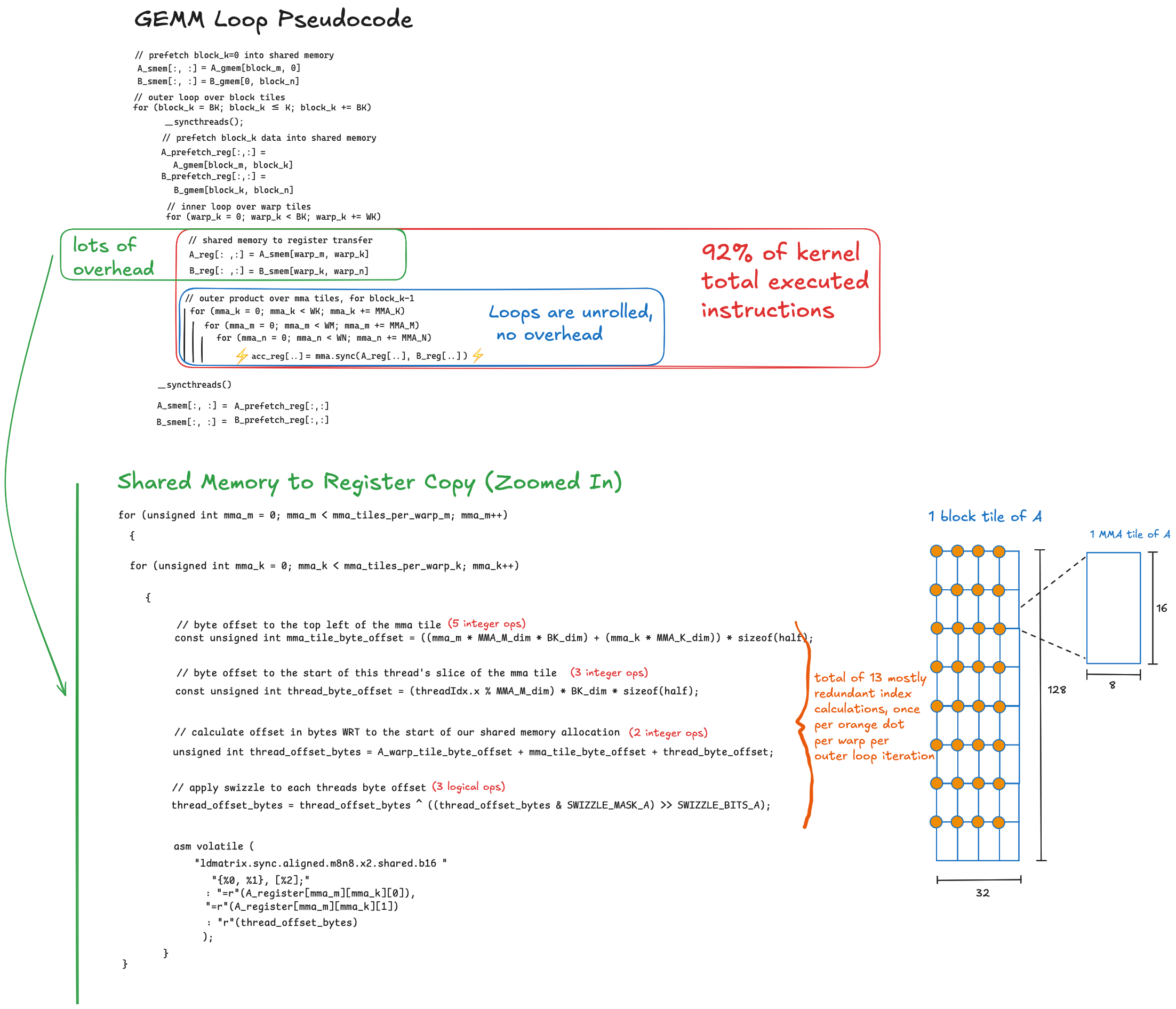
In order to make this more performant, we should move as much of this calculation as possible to happen at compile time, and whatever needs to happen at runtime should be as streamlined as possible. In the index calculation code shown above, fundamentally there are three distinct and dependent steps
- First each warp computes the memory address of the top left corner of the mma tile
- Each thread calculates the memory address of the element it will load, relative to (1)
- Because our shared memory layout is swizzled, each thread applies the swizzle function to the address computued in (2) in order to get the correct memory address in the swizzled layout.
All three steps are done for each of the 8x8 MMA tiles. Below is a visualization of this, the diagram below is a mini example where each MMA tile is four rows and one column, and each warp tile has 2x8 MMA tiles (using simpler examples like this allows us to make all the details as explicit as possible, and the ![]() is in the details).
is in the details).
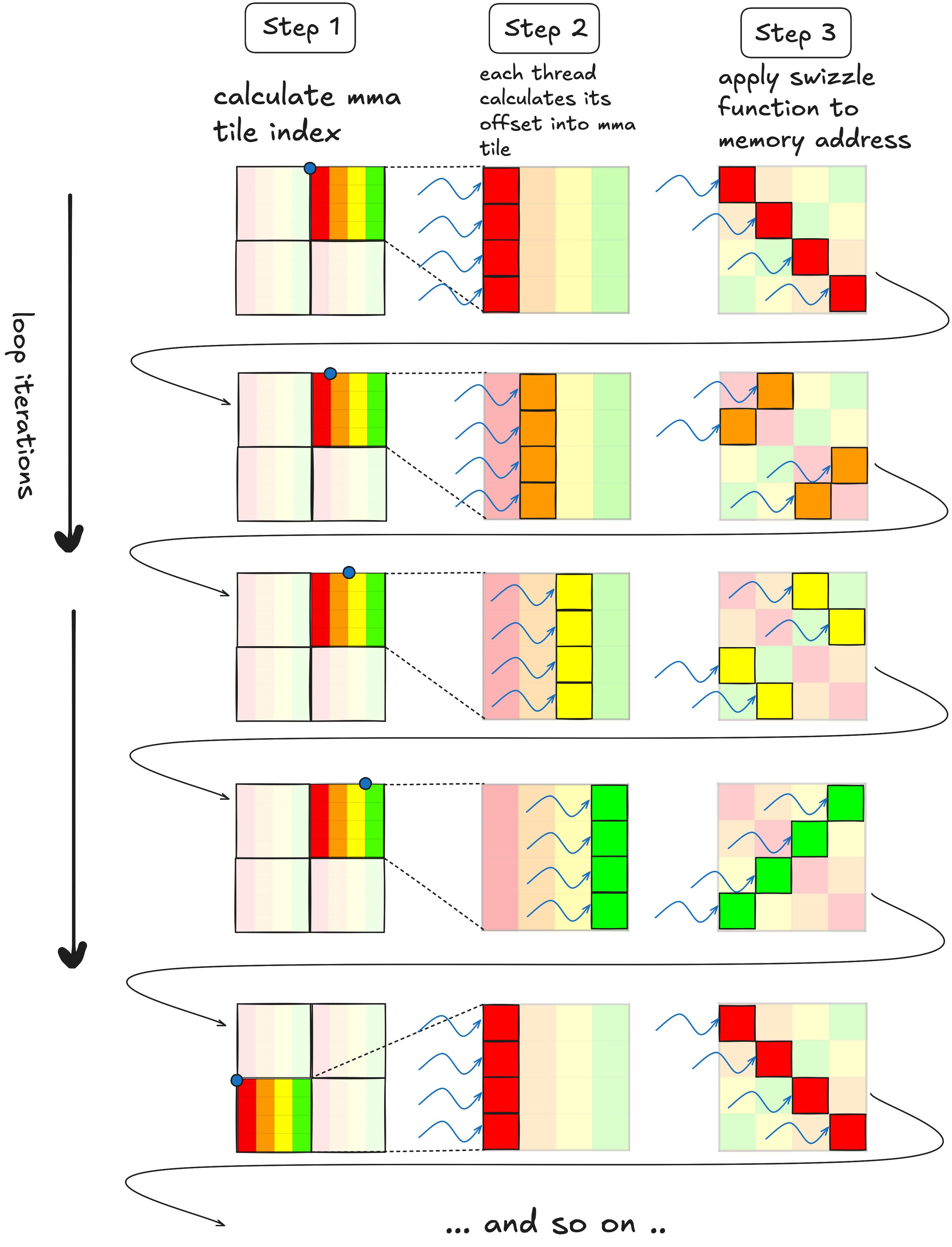
In the middle column, each thread has calculated the address of the value it is going to load, in the unswizzled layout. Each iteration, these pointers are advanced to the right by one column, until we get to the end of the warp tile at which point we go down to the next set of rows. If it weren’t for the swizzled layout, we could just advance the pointers by one each iteration, i.e. thread_row+=1. However, because the data is stored in a swizzled layout, advancing the pointers over to the next group of MMA tiles is not simply a matter of incrementing by one.
While incrementing by one will not work for iterating over a swizzled layout, we can achieve the equivalent effect by XORing each threads pointer with a constant.
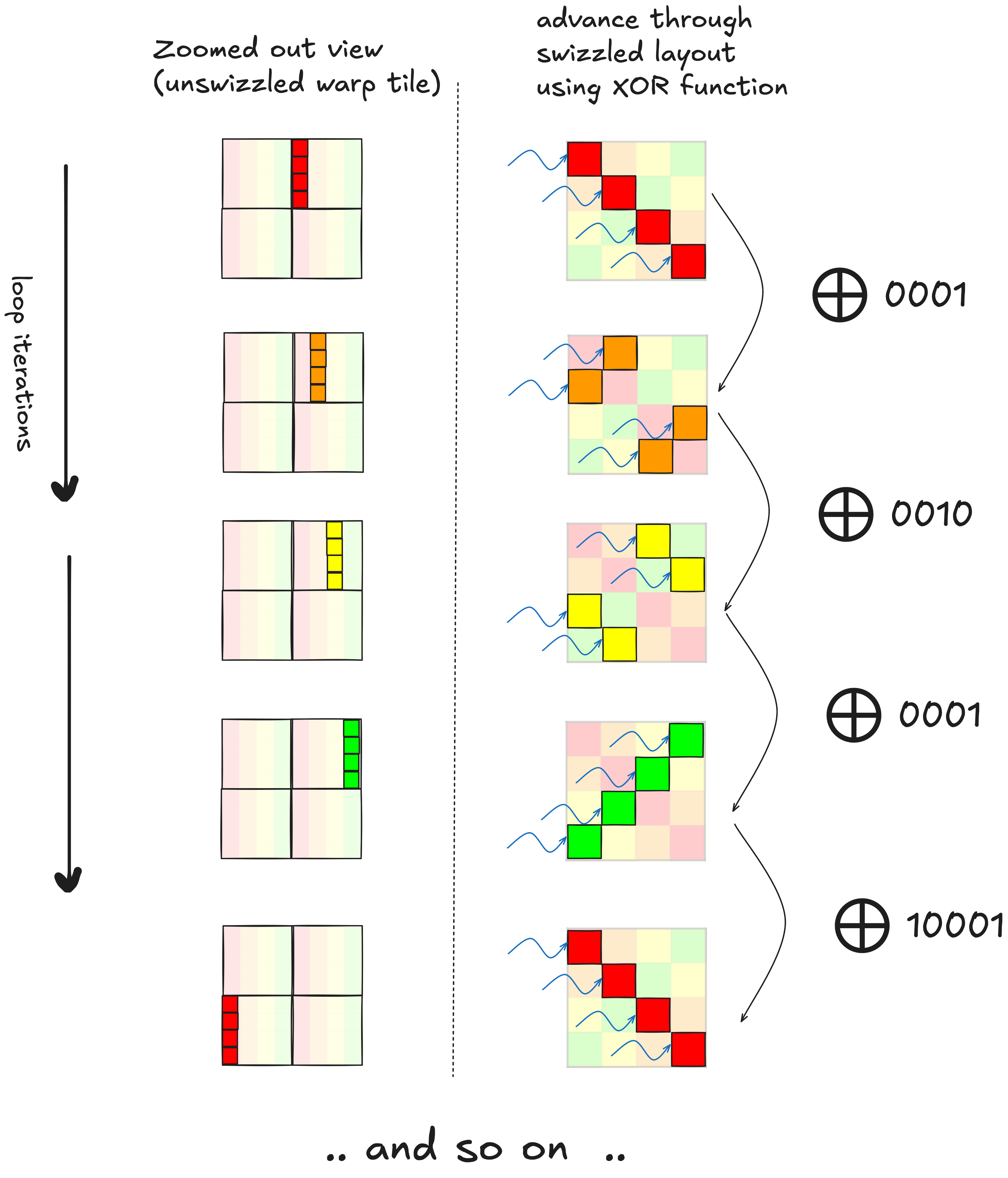 This reduces the amount of index calculation from ~13 operations in between each
 ldmatrix, down to a single XOR. After applying this optimization, the total number of instructions executed goes down to ~90M, which is slightly less than cuBLAS.
This illustrates the basic principle of efficiently iterating through a swizzled data layout. In the actual code, it is a bit more complicated because the swizzle function is more complicated, and we need to iterate through the tiles of A and B which have different dimensions from each other. Also the loops containing the ldmatrix instructions are manually unrolled, this makes the XORing easier, and also might allow the compiler to do a better job of interleaving the ldmatrix and mma.sync instructions to balance load between the two different pipelines.
The optimized index calcuation, loop unrolling, and adjusted tile dimensions are all implemented as part of the same kernel, that achieves a hard fought 1.2x speedup over the last one, and gets us to 86.7% of cuBLAS throughput.
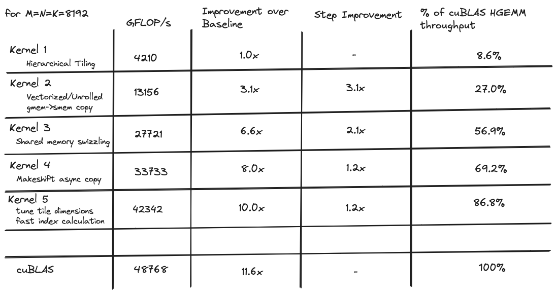
Kernel 6 - Double Buffering
Back to the profiler (for the last time). At this point many of the metrics between my kernel and cuBLAS were starting to look somewhat similiar. One thing that jumped out at me was that the threads in my kernel spend more time stalled on __syncthreads() than the cuBLAS kernel. At this point my kernel had a CPI (cycles per instruction) of 14, and about 2.6 of these cycles come from sychronization stalling. So this was not an egregious performance issue, but noticeable. A technique called double buffering enables you to remove one of the two __syncthreads() in the inner loop. After a bit of pondering I realized that this provides no guaruntee of a proportional decrease in cycles stalled on __syncthreads() (if you remove one __syncthreads(), threads might spend twice as much time stalled on the other). However, double buffering should also allow for a bit more instruction level parallelism inside the main loop, and it is implemented in CUTLASS kernels, and I had the shared memory to spare, so why not.
The data dependencies inside the main loop of our current GEMM kernel necessitate having two __syncthreads() in order to prevent race conditions in shared memory
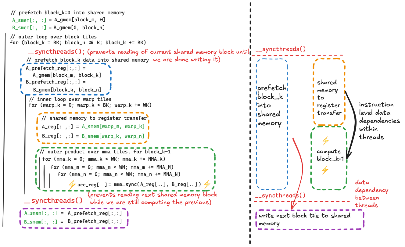 If we removed either, race conditions would occur because the thread to data mapping is different when writing to shared memory vs. reading it. This is because any given thread is computing on different values than the ones that it fetched from global memory and wrote to shared memory. This means that sychronization points are required to prevent race conditions, because the whole thread block must wait until all threads are done writing to shared memory before any thread starts reading from shared memory.
The cost of these sychronization points is less parallelism and potentially less hardware utilization. As the diagram above shows, there are four main components to the main loop.
- prefetching the next block tile into registers
- shared memory to register transfer in preparation for compute
- compute
- writing the prefetched data back from registers to shared memory
As the diagram above illustrates #4 is kept seperate from the other three because it involves writing to the data that is being read in #2, i.e. all 256 threads in a block must complete #2 before any start #4. This seperation is bad for performance, because it limits the compilers ability to interleave instructions of different types to balance load across different hardware pipelines.
The idea behind double buffering is that if we allocate an extra pair of shared memory buffers for the block tiles of $A$ and $B$, we can write to one pair of buffers concurrently with the other being read. This allows us to remove the second __syncthreads() from the mainloop. This should make things a bit faster.
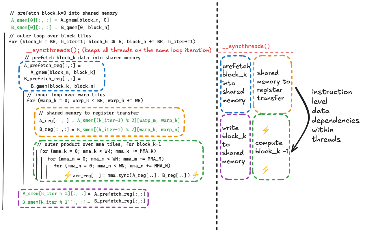
The two things that changed here are the removal of one of the __syncthreads(), and the addition of an index that we always use (%2) to track which of the two buffers is being read, and which is being written on any given iteration. The buffer that is being read and the buffer that is being written switches each iteration.
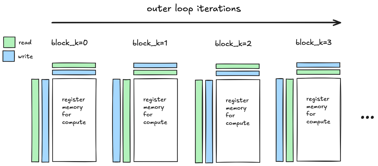
This results in a small speedup over the previous kernel. But at this stage of trying to optimize an already highly optimized kernel, I’ll take what I can get.

Conclusion
things I didn’t do
And this is where I called it a day! There are two avenues for further performance improvement, but the time I alloted to work on this ran out. The former is a lot easier than the latter.
-
optimized epiloge- As a reminder, the GEMM problem is $D=\alpha * A * B + \beta * C$. This is two computations stuffed into one kernel. The bulk of the compute is in the matrix multiplication $C^*=A * B$. Once we multiply the two matrices, then we do $D = \alpha * C^* + \beta * C$, this is generally referred to as the kernel epilogue. The former is an $O(N^3)$ problem, the later is $O(N^2)$. When N is large, the matrix multiplication dominates the runtime of the combined algorithm, when N is smaller the epilogue is more significant. The article focused entirely on the matrix multiplication, as this is the most interesting and important component of the GEMM problem. The kernel epilogue I used in all six kernels is innefficient - once the matrix multiplication is complete, the result is scattered across thread registers according to the
m16n8k8MMA layout (see below), and they are written directly back to memory. This write is uncoalesced and consequently achieves less than ideal bandwidth and latency. Improving this would likely narrow the gap between Kernel 6 and cuBLAS for smaller matrix sizes. - manual instruction mix tuning for inner loop- Projects like this and this match/exceed the performance of cuBLAS using custom built assemblers that allow them to write the kernel entirely in SASS. The inner loop of a GEMM kernel consists of shared memory loads and math instructions. If too many instructions of one type are grouped together, hardware pipelines will get overloaded and stall cycles will be incurred. If you want to write your kernels entirely in CUDA and PTX as I did, then instruction scheduling is the job of the compiler, the fact that I was able to get >90% of cuBLAS performance without any inlined assembly means that nvcc probably does a pretty good job at it. However, if one were really determined to write a kernel that is as fast or faster than cuBLAS for a range of matrix sizes, this would avenue would likely be necesssary.
performance on different matrix sizes
Here is a plot that shows the performance of the kernels I wrote, compared to cuBLAS, for a bunch of different matrix dimensions.
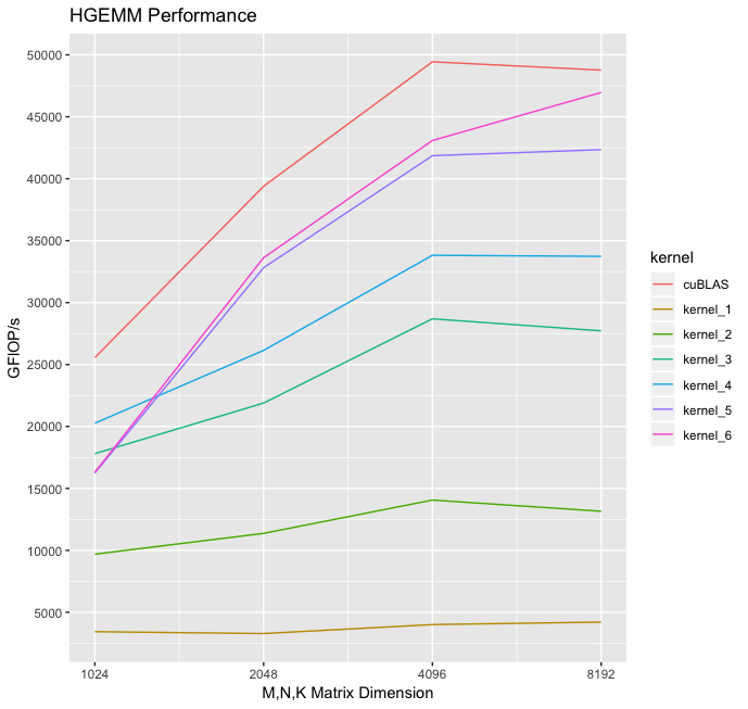
Note that the gap between the fastest kernel I wrote, and cuBLAS HGEMM is slightly larger for smaller matrices, possibly due to my unoptimized epilogue. Also possibly due to the fact that cuBLAS is selecting kernels that have been specifically tuned for those matrix dimensions.
lessons learned, newer GPUs are better
Given how many people and companies these days are buying NVIDIA GPUs almost exclusively for the purpose of running matrix multiplications, it seems like lots of work goes into improving the tensor cores in terms of programmability and performance between successive architectures. The tensor core throughput goes up by an order of magnitude with each new SM architecture, and the memory bandwidth also increases, but not proportionally.
In order to make the task of programming these powerful but imbalanced machines more manageable, the more recent Ampere and Hopper architectures introduced hardware support that enable several important parts of a GEMM kernel to run asychronously with respect to the rest of the SM. Ampere introduced hardware support for asychronous data copying from global memory to shared memory, I implemented a sort of hacked version of this using extra registers in Kernel 4. The Hopper architecture introduced something even fancier called the Tensor Memory Accelerator, which is essentially a copy engine that can perform index calculation, and initiate global memory transfers asychronously with respect to the rest of the SM. Thus developers writing kernels for Hopper probably dont have to worry about the efficiency of index calculation (like I did here), because this is offloaded to dedicated hardware in the TMA. Hopper also has asychronous tensor core instructions, that can read/write from/to shared memory, rather than registers (see here).
All of this asychronicity is a great thing for low occupancy, register hungry GEMM kernels. As discussed here, large arithmetic throughput means we need lots of fast memory to cache data, which means we cant run that many threads per SM, which means the GPU wont automatically hide our latency by context switching, which means we the programmer need to think more about how our latency is being hidden. This is where asychronicity is helpful.
All of this means that Hopper is kind of a new and different beast, if you look at GEMM kernels in CUTLASS that target Hopper the code has a different stucture than all of the other pre sm_90 kernels. Hopper kernels use a producer/consumer pattern, where a relatively small number of producer threads are initiating asynchronous data copies with the TMA, and then consumer threads are managing the tensor cores. I have never worked on kernels targetting Hopper so I dont know much about this at the moment, this article provides an interesting overview of the user experience of writing kernels for Hopper.
This is all to say that the kernels discussed here target the Turing architecture, which was SOTA in 2018, and if you are writing kernels targeting Ampere or Hopper, the techniques you employ for latency hiding will be different and easier. I used the Tesla T4 GPU because you can rent them on AWS for ~50 cents/hour, which is about as much money as I want to spend on EC2 instances. Using an older GPU was a blessing and a curse for this project, the curse was that no special hardware support was available for hiding memory latency on calculating indices, the blessing was that I had to do all this myself which was an educational experience!
Resources / Acknowledgements
Most of these resources have already been linked to in various places throughout this article, but I wanted to put them all in one place. These are some resources that have educated and inspired me, in no particular order
- I learned about the roofline model from Prof. Vuduc’s Intro to High Performance Computing class at Georgia Tech, all of the course videos are available here, these videos are an amazing free resource if you have the time and inclination to watch them. The part of this article about rooflines and computational intensity is similiar to what is presented in the “Basic Model of Locality” section.
- This article was a major source of inspiration for this project. Simon’s other articles are excellent as well, this is probably one of my favorite blogs on the internet at the moment.
- Another excellent blog about a systems view of ML. This article in particular is a very readable explanation of why things like memory bandwidth and arithmetic intensity matter when training neural nets on GPUs.
- Great article from a systems ML lab at stanford about the kernel engineering for the Hopper architecture.
- This is NVIDIA’s CUTLASS project, provides a bunch of abstractions that make it easier to write fast kernels.